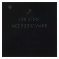
MCF5280CVM66 Freescale Semiconductor, MCF5280CVM66 Datasheet - Page 227

MCF5280CVM66
Manufacturer Part Number
MCF5280CVM66
Description
IC MPU 32BIT COLDF 256-MAPBGA
Manufacturer
Freescale Semiconductor
Series
MCF528xr
Datasheet
1.MCF5216CVM66J.pdf
(766 pages)
Specifications of MCF5280CVM66
Core Processor
Coldfire V2
Core Size
32-Bit
Speed
66MHz
Connectivity
CAN, EBI/EMI, Ethernet, I²C, SPI, UART/USART
Peripherals
DMA, LVD, POR, PWM, WDT
Number Of I /o
142
Program Memory Type
ROMless
Ram Size
64K x 8
Voltage - Supply (vcc/vdd)
2.7 V ~ 3.6 V
Data Converters
A/D 8x10b
Oscillator Type
External
Operating Temperature
-40°C ~ 85°C
Package / Case
256-MAPBGA
Controller Family/series
ColdFire
No. Of I/o's
150
Program Memory Size
2KB
Ram Memory Size
64KB
Cpu Speed
66.67MHz
Embedded Interface Type
CAN, I2C, SPI, UART
No. Of Pwm Channels
8
Rohs Compliant
Yes
Lead Free Status / RoHS Status
Lead free / RoHS Compliant
Eeprom Size
-
Program Memory Size
-
Available stocks
Company
Part Number
Manufacturer
Quantity
Price
Company:
Part Number:
MCF5280CVM66
Manufacturer:
FREESCAL
Quantity:
151
Company:
Part Number:
MCF5280CVM66
Manufacturer:
Freescale Semiconductor
Quantity:
10 000
Company:
Part Number:
MCF5280CVM66J
Manufacturer:
Freescale Semiconductor
Quantity:
10 000
Company:
Part Number:
MCF5280CVM66L
Manufacturer:
FREESCAL
Quantity:
151
- Current page: 227 of 766
- Download datasheet (9Mb)
The timing relationship of chip selects (CS[7:0]), byte selects (BS[3:0]), and output enable (OE) with
respect to CLKOUT is similar in that all transitions occur during the low phase of CLKOUT. However,
due to differences in on-chip signal routing, signals may not assert simultaneously.
13.4.1
When a bus cycle is initiated, the device first compares the address of that bus cycle with the base address
and mask configurations programmed for chip selects 0–7 (configured in CSCR0–CSCR7) and DRAM
block 0 and 1 address and control registers (configured in DACR0 and DACR1). If the driven address
compares with one of the programmed chip selects or DRAM blocks, the appropriate chip select is asserted
or the DRAM block is selected using the specifications programmed by the user in the respective
configuration register. Otherwise, the following occurs:
Table 13-2
Freescale Semiconductor
•
•
•
If the address and attributes do not match in CSCR or DACR, the processor runs an external
burst-inhibited bus cycle with a default of external termination on a 32-bit port.
Should an address and attribute match in multiple CSCRs, the matching chip-select signals are
driven; however, the processor runs an external burst-inhibited bus cycle with external termination
on a 32-bit port.
Should an address and attribute match both DACRs or a DACR and a CSCR, the operation is
undefined.
Bus Cycle Execution
shows the type of access as a function of match in the CSCRs and DACRs.
CLKOUT
CS[7:0]
BS[3:0]
Figure 13-2. Connections for External Memory Port Sizes
MCF5282 and MCF5216 ColdFire Microcontroller User’s Manual, Rev. 3
OE
Figure 13-3. Chip-Select Module Output Timing Diagram
Byte Enable
32-Bit Port
16-Bit Port
Processor
Data Bus
8-Bit Port
External
Memory
Memory
Memory
D[31:24]
Byte 0
Byte 0
Byte 2
Byte 0
Byte 1
Byte 2
Byte 3
BS3
D[23:16]
Byte 1
Byte 1
Byte 3
BS2
indeterminate values
Driven with
indeterminate values
D[15:8]
Byte 2
BS1
Driven with
Byte 3
D[7:0]
BS0
External Interface Module (EIM)
13-3
Related parts for MCF5280CVM66
Image
Part Number
Description
Manufacturer
Datasheet
Request
R
Part Number:
Description:
Manufacturer:
Freescale Semiconductor, Inc
Datasheet:
Part Number:
Description:
Manufacturer:
Freescale Semiconductor, Inc
Datasheet:
Part Number:
Description:
Manufacturer:
Freescale Semiconductor, Inc
Datasheet:
Part Number:
Description:
Manufacturer:
Freescale Semiconductor, Inc
Datasheet:
Part Number:
Description:
Manufacturer:
Freescale Semiconductor, Inc
Datasheet:
Part Number:
Description:
Manufacturer:
Freescale Semiconductor, Inc
Datasheet:
Part Number:
Description:
Manufacturer:
Freescale Semiconductor, Inc
Datasheet:
Part Number:
Description:
Manufacturer:
Freescale Semiconductor, Inc
Datasheet:
Part Number:
Description:
Manufacturer:
Freescale Semiconductor, Inc
Datasheet:
Part Number:
Description:
Manufacturer:
Freescale Semiconductor, Inc
Datasheet:
Part Number:
Description:
Manufacturer:
Freescale Semiconductor, Inc
Datasheet:
Part Number:
Description:
Manufacturer:
Freescale Semiconductor, Inc
Datasheet:
Part Number:
Description:
Manufacturer:
Freescale Semiconductor, Inc
Datasheet:
Part Number:
Description:
Manufacturer:
Freescale Semiconductor, Inc
Datasheet:
Part Number:
Description:
Manufacturer:
Freescale Semiconductor, Inc
Datasheet:


