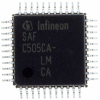
SAF-C515C-8EM CA Infineon Technologies, SAF-C515C-8EM CA Datasheet - Page 78

SAF-C515C-8EM CA
Manufacturer Part Number
SAF-C515C-8EM CA
Description
IC MCU 8BIT OTP MQFP-80-1
Manufacturer
Infineon Technologies
Series
C5xx/C8xxr
Datasheet
1.SAF-C515C-8EM_CA.pdf
(96 pages)
Specifications of SAF-C515C-8EM CA
Core Processor
C500
Core Size
8-Bit
Speed
10MHz
Connectivity
CAN, EBI/EMI, SPI, UART/USART
Peripherals
POR, PWM, WDT
Number Of I /o
49
Program Memory Size
64KB (64K x 8)
Program Memory Type
OTP
Ram Size
2.5K x 8
Voltage - Supply (vcc/vdd)
4.25 V ~ 5.5 V
Data Converters
A/D 8x10b
Oscillator Type
External
Operating Temperature
-40°C ~ 85°C
Package / Case
80-SQFP
Data Bus Width
8 bit
Data Ram Size
2.25 KB
Interface Type
USART, SSC
Maximum Clock Frequency
10 MHz
Number Of Programmable I/os
49
Number Of Timers
3
Operating Supply Voltage
5 V
Maximum Operating Temperature
+ 85 C
Mounting Style
SMD/SMT
Minimum Operating Temperature
- 40 C
On-chip Adc
10 bit, 8 Channel
Packages
PG-MQFP-80
Max Clock Frequency
10.0 MHz
Sram (incl. Cache)
2.25 KByte
Can Nodes
1
A / D Input Lines (incl. Fadc)
8
Program Memory
64.0 KByte
Lead Free Status / RoHS Status
Lead free / RoHS Compliant
Eeprom Size
-
Lead Free Status / Rohs Status
Details
Other names
F515C8EMCANP
F515C8EMCAXT
SAF-C515C-8EMCA
SAF-C515C-8EMCA
SAF-C515C-8EMCAIN
SAFC515C8EMCAX
SP000068749
SP000106399
F515C8EMCAXT
SAF-C515C-8EMCA
SAF-C515C-8EMCA
SAF-C515C-8EMCAIN
SAFC515C8EMCAX
SP000068749
SP000106399
A/D Converter Characteristics (Operating Conditions apply)
Parameter
Analog input voltage
Sample time
Conversion cycle time
Total unadjusted error
Internal resistance of
reference voltage source
Internal resistance of
analog source
ADC input capacitance
1)
2)
3)
4)
5)
6)
Data Sheet
V
these cases will be X000
During the sample time the input capacitance
internal resistance of the analog source must allow the capacitance to reach their final voltage level within
After the end of the sample time
This parameter includes the sample time
calibration. Values for the conversion clock
the previous page.
T
other voltages within the defined voltage range.
If an overload condition occurs on maximum 2 not selected analog input pins and the absolute sum of input
overload currents on all analog input pins does not exceed 10 mA, an additional conversion error of 1/2 LSB
is permissible.
During the conversion the ADC’s capacitance must be repeatedly charged or discharged. The internal
resistance of the reference source must allow the capacitance to reach their final voltage level within the
indicated time. The maximum internal resistance results from the programmed conversion timing.
Not 100% tested, but guaranteed by design characterization.
UE
AIN
is tested at
may exceed
V
AREF
V
AGND
= 5.0 V,
H
or
or X3FF
V
AREF
Symbol
V
t
t
T
R
R
C
t
S
ADCC
V
S
UE
AIN
AREF
ASRC
AIN
, changes of the analog input voltage have no effect on the conversion result.
AGND
H
up to the absolute maximum ratings. However, the conversion result in
, respectively.
= 0 V,
t
S
t
min.
V
–
–
–
–
–
–
ADC
, the time for determining the digital result and the time for the
AGND
V
C
DD
AIN
depend on programming and can be taken from the table on
Limit Values
= 4.9 V. It is guaranteed by design characterization for all
74
can be charged/discharged by the external source. The
max.
V
16
8
96
48
t
- 0.25
t
- 0.25
50
ADC
S
2
AREF
/ 500
t
IN
t
t
t
/ 250
IN
IN
IN
Unit Test Condition
V
ns
ns
LSB
k
k
pF
1)
Prescaler
Prescaler
Prescaler
Prescaler
4)
t
t
6)
ADC
S
in [ns]
in [ns]
2)6)
5)6)
8
4
8
4
C515C
2003-02
2)
3)
t
S
.


