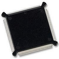
MC68HC16Z1CEH25 Freescale Semiconductor, MC68HC16Z1CEH25 Datasheet - Page 438

MC68HC16Z1CEH25
Manufacturer Part Number
MC68HC16Z1CEH25
Description
IC MCU 16BIT 25MHZ 132-PQFP
Manufacturer
Freescale Semiconductor
Series
HC16r
Datasheet
1.MC68HC16Z1VEH16.pdf
(500 pages)
Specifications of MC68HC16Z1CEH25
Core Processor
CPU16
Core Size
16-Bit
Speed
25MHz
Connectivity
EBI/EMI, SCI, SPI
Peripherals
POR, PWM, WDT
Number Of I /o
16
Program Memory Type
ROMless
Ram Size
1K x 8
Voltage - Supply (vcc/vdd)
2.7 V ~ 5.5 V
Data Converters
A/D 8x10b
Oscillator Type
Internal
Operating Temperature
-40°C ~ 85°C
Package / Case
132-QFP
Package
132PQFP
Family Name
HC16
Maximum Speed
25 MHz
Operating Supply Voltage
3.3|5 V
Data Bus Width
16 Bit
Number Of Programmable I/os
16
On-chip Adc
8-chx10-bit
Number Of Timers
11
Controller Family/series
68HC16
No. Of I/o's
16
Ram Memory Size
1KB
Cpu Speed
25MHz
No. Of Timers
2
Embedded Interface Type
QSPI, SCI
Rohs Compliant
Yes
Processor Series
HC16Z
Core
CPU16
Data Ram Size
1 KB
Interface Type
SCI, SPI, UART
Maximum Clock Frequency
25 MHz
Maximum Operating Temperature
+ 85 C
Mounting Style
SMD/SMT
Minimum Operating Temperature
- 40 C
Lead Free Status / RoHS Status
Lead free / RoHS Compliant
Eeprom Size
-
Program Memory Size
-
Lead Free Status / Rohs Status
Details
Available stocks
Company
Part Number
Manufacturer
Quantity
Price
Company:
Part Number:
MC68HC16Z1CEH25
Manufacturer:
Freescale Semiconductor
Quantity:
135
Company:
Part Number:
MC68HC16Z1CEH25
Manufacturer:
Freescale Semiconductor
Quantity:
10 000
- Current page: 438 of 500
- Download datasheet (6Mb)
D.7.13 SPI Control Register
SPCR — SPI Control Register
SPIE — SPI Interrupt Enable
SPE — SPI Enable
WOMP — Wired-OR Mode for SPI Pins
MSTR — Master/Slave Mode Select
CPOL — Clock Polarity
CPHA — Clock Phase
LSBF — Least Significant Bit First
D-64
RESET:
SPIE
15
0
The SPCR contains parameters for configuring the SPI. The register can be read or
written at any time.
CPOL is used to determine the inactive state of the serial clock (SCK). It is used with
CPHA to produce a desired clock/data relationship between master and slave devices.
CPHA determines which edge of SCK causes data to change and which edge causes
data to be captured. CPHA is used with CPOL to produce a desired clock/data rela-
tionship between master and slave devices.
0 = SPI interrupts disabled.
1 = SPI interrupts enabled.
0 = SPI is disabled.
1 = SPI is enabled.
0 = Outputs have normal CMOS drivers.
1 = Pins designated for output by MDDR have open-drain drivers, regardless of
0 = SPI is a slave device.
1 = SPI is system master.
0 = The inactive state value of SCK is logic level zero.
1 = The inactive state value of SCK is logic level one.
0 = Data captured on the leading edge of SCK and changed on the trailing edge of
1 = Data is changed on the leading edge of SCK and captured on the trailing edge
0 = Serial data transfer starts with LSB.
1 = Serial data transfer starts with MSB.
SPE
14
0
whether the pins are used as SPI outputs or for general-purpose I/O, and re-
gardless of whether the SPI is enabled.
SCK.
of SCK.
WOMP
13
0
MSTR
12
0
Freescale Semiconductor, Inc.
CPOL
11
For More Information On This Product,
0
CPHA
10
0
Go to: www.freescale.com
REGISTER SUMMARY
LSBF
9
0
SIZE
8
1
7
0
6
0
5
0
4
0
SPBR[7:0]
3
0
M68HC16 Z SERIES
USER’S MANUAL
2
1
$YFFC38
1
0
0
0
Related parts for MC68HC16Z1CEH25
Image
Part Number
Description
Manufacturer
Datasheet
Request
R
Part Number:
Description:
Manufacturer:
Freescale Semiconductor, Inc
Datasheet:
Part Number:
Description:
Manufacturer:
Freescale Semiconductor, Inc
Datasheet:
Part Number:
Description:
Manufacturer:
Freescale Semiconductor, Inc
Datasheet:
Part Number:
Description:
Manufacturer:
Freescale Semiconductor, Inc
Datasheet:
Part Number:
Description:
Manufacturer:
Freescale Semiconductor, Inc
Datasheet:
Part Number:
Description:
Manufacturer:
Freescale Semiconductor, Inc
Datasheet:
Part Number:
Description:
Manufacturer:
Freescale Semiconductor, Inc
Datasheet:
Part Number:
Description:
Manufacturer:
Freescale Semiconductor, Inc
Datasheet:
Part Number:
Description:
Manufacturer:
Freescale Semiconductor, Inc
Datasheet:
Part Number:
Description:
Manufacturer:
Freescale Semiconductor, Inc
Datasheet:
Part Number:
Description:
Manufacturer:
Freescale Semiconductor, Inc
Datasheet:
Part Number:
Description:
Manufacturer:
Freescale Semiconductor, Inc
Datasheet:
Part Number:
Description:
Manufacturer:
Freescale Semiconductor, Inc
Datasheet:
Part Number:
Description:
Manufacturer:
Freescale Semiconductor, Inc
Datasheet:
Part Number:
Description:
Manufacturer:
Freescale Semiconductor, Inc
Datasheet:


