M68EVB908GB60E Freescale Semiconductor, M68EVB908GB60E Datasheet - Page 272
M68EVB908GB60E
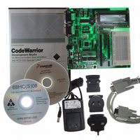
Manufacturer Part Number
M68EVB908GB60E
Description
BOARD EVAL FOR MC9S08GB60
Manufacturer
Freescale Semiconductor
Type
MCUr
Datasheet
1.M68EVB908GB60E.pdf
(290 pages)
Specifications of M68EVB908GB60E
Contents
Module and Misc Hardware
Processor To Be Evaluated
MC9S08GB
Data Bus Width
8 bit
Interface Type
RS-232
Silicon Manufacturer
Freescale
Core Architecture
HCS08
Core Sub-architecture
HCS08
Silicon Core Number
MC9S08
Silicon Family Name
S08GB
Kit Contents
GB60 Evaluation Kit
Rohs Compliant
Yes
For Use With/related Products
MC9S08GB60
Lead Free Status / RoHS Status
Lead free / RoHS Compliant


Appendix A Electrical Characteristics
272
1
2
3
4
5
6
7
8
Output clock ICGOUT frequency
Minimum DCO clock (ICGDCLK) frequency
Maximum DCO clock (ICGDCLK) frequency
Self-clock mode (ICGOUT) frequency
Self-clock mode reset (ICGOUT) frequency
Loss of reference frequency
Loss of DCO frequency
Crystal start-up time
FLL lock time
FLL frequency unlock range
FLL frequency lock range
ICGOUT period jitter,
Internal oscillator deviation from trimmed frequency
Self-clocked mode frequency is the frequency that the DCO generates when the FLL is open-loop.
Loss of reference frequency is the reference frequency detected internally, which transitions the ICG into self-clocked
mode if it is not in the desired range.
Loss of DCO frequency is the DCO frequency detected internally, which transitions the ICG into FLL bypassed external
mode (if an external reference exists) if it is not in the desired range.
This parameter is characterized before qualification rather than 100% tested.
Proper PC board layout procedures must be followed to achieve specifications.
This specification applies to the period of time required for the FLL to lock after entering FLL engaged internal or external
modes. If a crystal/resonator is being used as the reference, this specification assumes it is already running.
Jitter is the average deviation from the programmed frequency measured over the specified interval at maximum f
Measurements are made with the device powered by filtered supplies and clocked by a stable external clock signal. Noise
injected into the FLL circuitry via V
percentage for a given interval.
See
CLKS = 10, REFS = 0
All other cases
Low range
High range
Low range
High range
Low range
High range
Long term jitter (averaged over 2 ms interval)
V
V
DD
DD
Figure A-10
= 1.8 – 3.6 V, (constant temperature)
= 3.0 V ±10%, –40° C to 85° C
4, 6
(V
DDA
Characteristic
4, 5
4, 7
= V
3
measured at f
DDA
2
Table A-9. ICG Frequency Specifications (continued)
(min) to V
DDA
1
ICGOUT
and V
MC9S08GB/GT Data Sheet, Rev. 2.3
DDA
Max
SSA
(max), Temperature Range = –40 to 85°C Ambient)
and variation in crystal oscillator frequency increase the C
8
f
f
ICGDCLKmax
ICGDCLKmin
f
Symbol
f
Self_reset
n
ACC
ICGOUT
t
t
C
t
n
t
CSTH
f
f
CSTL
Lockh
Unlock
f
Lockl
LOR
LOD
Self
Lock
Jitter
int
f
f
ICGDCLKmin
Extal
f
lo
–4*N
–2*N
Min
5.5
0.5
(min)
50
—
—
—
—
—
—
—
8
5
(min)
Typical
± 0.5
±0.5
430
—
—
8
4
Freescale Semiconductor
f
f
f
ICGDCLKmax
ICGDCLKmax
Extal
(max)
Max
10.5
500
4*N
2*N
1.5
0.2
40
25
±2
±2
—
—
2
2
(max)
Jitter
counts
counts
% f
ICGOUT
MHz
MHz
MHz
MHz
MHz
MHz
Unit
kHz
ms
ms
%
ICG
.
Related parts for M68EVB908GB60E
Image
Part Number
Description
Manufacturer
Datasheet
Request
R

Part Number:
Description:
Manufacturer:
Freescale Semiconductor, Inc
Datasheet:
Part Number:
Description:
Manufacturer:
Freescale Semiconductor, Inc
Datasheet:
Part Number:
Description:
Manufacturer:
Freescale Semiconductor, Inc
Datasheet:
Part Number:
Description:
Manufacturer:
Freescale Semiconductor, Inc
Datasheet:
Part Number:
Description:
Manufacturer:
Freescale Semiconductor, Inc
Datasheet:
Part Number:
Description:
Manufacturer:
Freescale Semiconductor, Inc
Datasheet:
Part Number:
Description:
Manufacturer:
Freescale Semiconductor, Inc
Datasheet:
Part Number:
Description:
Manufacturer:
Freescale Semiconductor, Inc
Datasheet:
Part Number:
Description:
Manufacturer:
Freescale Semiconductor, Inc
Datasheet:
Part Number:
Description:
Manufacturer:
Freescale Semiconductor, Inc
Datasheet:
Part Number:
Description:
Manufacturer:
Freescale Semiconductor, Inc
Datasheet:
Part Number:
Description:
Manufacturer:
Freescale Semiconductor, Inc
Datasheet:
Part Number:
Description:
Manufacturer:
Freescale Semiconductor, Inc
Datasheet:
Part Number:
Description:
Manufacturer:
Freescale Semiconductor, Inc
Datasheet:
Part Number:
Description:
Manufacturer:
Freescale Semiconductor, Inc
Datasheet: