C8051F336DK Silicon Laboratories Inc, C8051F336DK Datasheet - Page 8
C8051F336DK
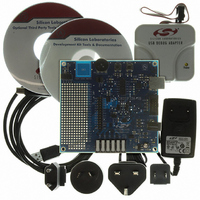
Manufacturer Part Number
C8051F336DK
Description
DEV KIT FOR C8051F336
Manufacturer
Silicon Laboratories Inc
Type
MCUr
Specifications of C8051F336DK
Contents
Evaluation Board, Power Supply, USB Cables, Adapter and Documentation
Processor To Be Evaluated
C8051F33x
Interface Type
USB, UART
Operating Supply Voltage
7 V to 15 V
Lead Free Status / RoHS Status
Lead free / RoHS Compliant
For Use With/related Products
C8051F336
Lead Free Status / Rohs Status
Lead free / RoHS Compliant
Other names
336-1430


C8051F336/7/8/9
15. Interrupts
16. Flash Memory
17. Reset Sources
18. Power Management Modes
19. Oscillators and Clock Selection
20. Port Input/Output
21. SMBus
22. UART0
23. Enhanced Serial Peripheral Interface (SPI0)
8
Figure 16.1. Security Byte Decoding ....................................................................... 93
Figure 17.1. Reset Sources ................................................................................... 100
Figure 17.2. Power-On and VDD Monitor Reset Timing ....................................... 101
Figure 19.1. Oscillator Options .............................................................................. 109
Figure 19.2. External 32.768 kHz Quartz Crystal Oscillator Connection Diagram 117
Figure 20.1. Port I/O Functional Block Diagram .................................................... 119
Figure 20.2. Port I/O Cell Block Diagram .............................................................. 121
Figure 20.3. Port I/O Overdrive Current ................................................................ 121
Figure 20.4. Crossbar Priority Decoder - Possible Pin Assignments .................... 124
Figure 20.5. Crossbar Priority Decoder Example .................................................. 125
Figure 21.1. SMBus Block Diagram ...................................................................... 138
Figure 21.2. Typical SMBus Configuration ............................................................ 139
Figure 21.3. SMBus Transaction ........................................................................... 140
Figure 21.4. Typical SMBus SCL Generation ........................................................ 142
Figure 21.5. Typical Master Write Sequence ........................................................ 151
Figure 21.6. Typical Master Read Sequence ........................................................ 152
Figure 21.7. Typical Slave Write Sequence .......................................................... 153
Figure 21.8. Typical Slave Read Sequence .......................................................... 154
Figure 22.1. UART0 Block Diagram ...................................................................... 159
Figure 22.2. UART0 Baud Rate Logic ................................................................... 160
Figure 22.3. UART Interconnect Diagram ............................................................. 161
Figure 22.4. 8-Bit UART Timing Diagram .............................................................. 161
Figure 22.5. 9-Bit UART Timing Diagram .............................................................. 162
Figure 22.6. UART Multi-Processor Mode Interconnect Diagram ......................... 163
Figure 23.1. SPI Block Diagram ............................................................................ 167
Figure 23.2. Multiple-Master Mode Connection Diagram ...................................... 169
Figure 23.3. 3-Wire Single Master and 3-Wire Single Slave Mode Connection Diagram
Figure 23.4. 4-Wire Single Master Mode and 4-Wire Slave Mode Connection Diagram
Figure 23.5. Master Mode Data/Clock Timing ....................................................... 172
Figure 23.6. Slave Mode Data/Clock Timing (CKPHA = 0) ................................... 172
Figure 23.7. Slave Mode Data/Clock Timing (CKPHA = 1) ................................... 173
Figure 23.8. SPI Master Timing (CKPHA = 0) ....................................................... 177
Figure 23.9. SPI Master Timing (CKPHA = 1) ....................................................... 177
Figure 23.10. SPI Slave Timing (CKPHA = 0) ....................................................... 178
170
170
Rev.1.0
Related parts for C8051F336DK
Image
Part Number
Description
Manufacturer
Datasheet
Request
R

Part Number:
Description:
SMD/C°/SINGLE-ENDED OUTPUT SILICON OSCILLATOR
Manufacturer:
Silicon Laboratories Inc
Part Number:
Description:
Manufacturer:
Silicon Laboratories Inc
Datasheet:
Part Number:
Description:
N/A N/A/SI4010 AES KEYFOB DEMO WITH LCD RX
Manufacturer:
Silicon Laboratories Inc
Datasheet:
Part Number:
Description:
N/A N/A/SI4010 SIMPLIFIED KEY FOB DEMO WITH LED RX
Manufacturer:
Silicon Laboratories Inc
Datasheet:
Part Number:
Description:
N/A/-40 TO 85 OC/EZLINK MODULE; F930/4432 HIGH BAND (REV E/B1)
Manufacturer:
Silicon Laboratories Inc
Part Number:
Description:
EZLink Module; F930/4432 Low Band (rev e/B1)
Manufacturer:
Silicon Laboratories Inc
Part Number:
Description:
I°/4460 10 DBM RADIO TEST CARD 434 MHZ
Manufacturer:
Silicon Laboratories Inc
Part Number:
Description:
I°/4461 14 DBM RADIO TEST CARD 868 MHZ
Manufacturer:
Silicon Laboratories Inc
Part Number:
Description:
I°/4463 20 DBM RFSWITCH RADIO TEST CARD 460 MHZ
Manufacturer:
Silicon Laboratories Inc
Part Number:
Description:
I°/4463 20 DBM RADIO TEST CARD 868 MHZ
Manufacturer:
Silicon Laboratories Inc
Part Number:
Description:
I°/4463 27 DBM RADIO TEST CARD 868 MHZ
Manufacturer:
Silicon Laboratories Inc
Part Number:
Description:
I°/4463 SKYWORKS 30 DBM RADIO TEST CARD 915 MHZ
Manufacturer:
Silicon Laboratories Inc
Part Number:
Description:
N/A N/A/-40 TO 85 OC/4463 RFMD 30 DBM RADIO TEST CARD 915 MHZ
Manufacturer:
Silicon Laboratories Inc
Part Number:
Description:
I°/4463 20 DBM RADIO TEST CARD 169 MHZ
Manufacturer:
Silicon Laboratories Inc