C8051F336DK Silicon Laboratories Inc, C8051F336DK Datasheet
C8051F336DK
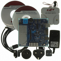
Specifications of C8051F336DK


Related parts for C8051F336DK

C8051F336DK Summary of contents
Page 1
... Keil 8051 Development Tools (macro assembler, linker, evaluation ‘C’ compiler) Other useful software that is provided in the CD-ROM includes: Configuration Wizard 2 Keil uVision Drivers CP210x USB to UART Virtual COM Port (VCP) Drivers Rev. 0.2 8/ ’ Copyright © 2007 by Silicon Laboratories C8051F336DK ...
Page 2
... C8051F336DK 3.1. Software Installation The included CD-ROM contains the Silicon Laboratories Integrated Development Environment (IDE), Keil software 8051 tools and additional documentation. Insert the CD-ROM into your PC’s CD-ROM drive. An installer will automatically launch, allowing you to install the IDE software or read documentation by clicking buttons on the Installation Panel ...
Page 3
... In just a few steps, the wizard creates complete startup code for a specific Silicon Laboratories MCU. The program is configurable to provide the output assembly. For more information, please refer to the Configuration Wizard 2 help available under the Help menu in Config Wizard 2. C8051F336DK Rev. 0.2 3 ...
Page 4
... C8051F336DK 4.4. Keil uVision2 and uVision3 Silicon Laboratories Drivers As an alternative to the Silicon Laboratories IDE, the uVision debug driver allows the Keil uVision IDE to communicate with Silicon Laboratories on-chip debug logic. In-system Flash memory programming integrated into the driver allows for rapidly updating target code. The uVision IDE can be used to start and stop program execution, set breakpoints, check variables, inspect and modify memory contents, and single-step through programs running on the actual target hardware ...
Page 5
... Right-click on “New Project” in the Project Window. Select Add Groups to project. Add pre-defined groups or add customized groups. Right-click on the group name and choose Add file to group. Select files to be added. Continue adding files until all project files have been added. C8051F336DK Rev. 0.2 5 ...
Page 6
... C8051F336DK 6.2. Building and Downloading the Program for Debugging 1. Once all source files have been added to the target build, build the project by clicking on the Build/Make Project button in the toolbar or selecting Project Note: After the project has been built the first time, the Build/Make Project command will only build the files that have been changed since the previous build ...
Page 7
... Analog I/O terminal block Pin 2 J11 SW3 Pin 1 P0.7 RESET R14 Pin P1.3 D7 Pin 1 Pin 2 Pin F338 SILICON LABS www.silabs.com TB1 +3VD GND Pin 1 Prototype Area I/O Connection Points Figure 3. C8051F338 Target Board Rev. 0.2 C8051F336DK P2 USB D4 CP 2102 U3 J4 J10 Pin 1 Pin PWR 7 ...
Page 8
... C8051F336DK 8.1. Target Board Shorting Blocks: Factory Defaults The C8051F338 target board comes from the factory with pre-installed shorting blocks on many headers. Figure 4 shows the positions of the factory default shorting blocks. Pin 2 J11 SW3 Pin 1 Figure 4. C8051F338 Target Board Shorting Blocks: Factory Defaults 8 P0 ...
Page 9
... C13 and C14 using values appropriate for the crystal you select. If you wish to operate the external oscillator in capacitor or RC mode, options to install a capacitor network are also available on the target board. Populate C14 for capacitor mode, and populate R7 and C14 for RC mode. Refer to the C8051F336/7/8/9 data sheet for more information on the use of external oscillators. C8051F336DK Rev. 0.2 9 ...
Page 10
... C8051F336DK 8.4. Switches and LEDs Two push-button switches are provided on the target board. Switch SW1 is connected to the RESET pin of the C8051F338. Pressing SW1 puts the device into its hardware-reset state. Switch SW2 is connected to the C8051F338’s general purpose I/O (GPIO) pin through headers. Pressing SW2 generates a logic low signal on the port pin ...
Page 11
... P0.3 19 P0.4 20 P0.5 21 P0.6 22 P0.7 23 P1.0 24 P1.1 25 P1.2 26 Pin # Description (+3.3 VDC GND (Ground) 4 P2.4/C2D 5 /RST (Reset) 6 P2.4 7 /RST/C2CK 8 Not Connected 10 USB Power (+5VDC from J4) Rev. 0.2 C8051F336DK P1.3 P1.4 P1.5 P1.6 P1.7 P2.0 P2.1 P2.2 P2.3 P2.4 /RST GND GND 11 ...
Page 12
... C8051F336DK 8.7. Serial Interface (J3) A USB-to-UART bridge circuit (U3) and USB connector (P2) are provided on the target board to facilitate serial connections to UART0 of the C8051F338. The Silicon Labs CP2102 (U3) USB-to-UART bridge provides data connectivity between the C8051F338 and the PC via a USB port. The TX, RX, RTS and CTS signals of UART0 may be connected to the CP2102 by installing shorting blocks on header J3 ...
Page 13
... P1.7 P2.0 P2.1 P2.2 P2.3 P2.4 C2D P2.4/C2D /RST C2CK /RST/C2CK VDD GND Rev. 0.2 C8051F336DK Relevant Headers VREF J1[3], TB1[6]*, J5[1] IDAC J1[4], J1[2]*, TB1[2], J6[1] XTAL1 J1[5]*, J9[2] XTAL2 J1[6]*, J10[2] J1[7], J3[5] J1[8], J3[7] J1[9], TB1[1] J1[10], J3[3] ...
Page 14
... C8051F336DK 9. Schematics 14 Rev. 0.2 ...
Page 15
... C8051F336DK Rev. 0.2 15 ...
Page 16
... C8051F336DK C I ONTACT NFORMATION Silicon Laboratories Inc. 400 West Cesar Chavez Austin, TX 78701 Tel: 1+(512) 416-8500 Fax: 1+(512) 416-9669 Toll Free: 1+(877) 444-3032 Email: MCUinfo@silabs.com Internet: www.silabs.com The information in this document is believed to be accurate in all respects at the time of publication but is subject to change without notice. ...