C8051F336DK Silicon Laboratories Inc, C8051F336DK Datasheet - Page 101
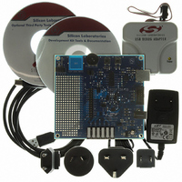
C8051F336DK
Manufacturer Part Number
C8051F336DK
Description
DEV KIT FOR C8051F336
Manufacturer
Silicon Laboratories Inc
Type
MCUr
Specifications of C8051F336DK
Contents
Evaluation Board, Power Supply, USB Cables, Adapter and Documentation
Processor To Be Evaluated
C8051F33x
Interface Type
USB, UART
Operating Supply Voltage
7 V to 15 V
Lead Free Status / RoHS Status
Lead free / RoHS Compliant
For Use With/related Products
C8051F336
Lead Free Status / Rohs Status
Lead free / RoHS Compliant
Other names
336-1430


17.1. Power-On Reset
During power-up, the device is held in a reset state and the RST pin is driven low until V
V
increases (V
power-on and V
cause the device to be released from reset before V
1 ms, the power-on reset delay (T
On exit from a power-on reset, the PORSF flag (RSTSRC.1) is set by hardware to logic 1. When PORSF is
set, all of the other reset flags in the RSTSRC Register are indeterminate (PORSF is cleared by all other
resets). Since all resets cause program execution to begin at the same location (0x0000) software can
read the PORSF flag to determine if a power-up was the cause of reset. The content of internal data mem-
ory should be assumed to be undefined after a power-on reset. The V
power-on reset.
RST
. A delay occurs before the device is released from reset; the delay decreases as the V
DD
Logic HIGH
DD
Logic LOW
ramp time is defined as how fast V
Figure 17.2. Power-On and V
2.70
2.55
2.0
1.0
monitor reset timing. The maximum V
/RST
V
RST
PORDelay
Power-On
Reset
) is typically less than 0.3 ms.
T
PORDelay
Rev.1.0
DD
DD
DD
reaches the V
ramps from 0 V to V
DD
Monitor Reset Timing
ramp time is 1 ms; slower ramp times may
Monitor
Reset
VDD
RST
C8051F336/7/8/9
DD
level. For ramp times less than
monitor is enabled following a
RST
). Figure 17.2. plots the
VDD
DD
t
settles above
DD
ramp time
101
Related parts for C8051F336DK
Image
Part Number
Description
Manufacturer
Datasheet
Request
R

Part Number:
Description:
SMD/C°/SINGLE-ENDED OUTPUT SILICON OSCILLATOR
Manufacturer:
Silicon Laboratories Inc
Part Number:
Description:
Manufacturer:
Silicon Laboratories Inc
Datasheet:
Part Number:
Description:
N/A N/A/SI4010 AES KEYFOB DEMO WITH LCD RX
Manufacturer:
Silicon Laboratories Inc
Datasheet:
Part Number:
Description:
N/A N/A/SI4010 SIMPLIFIED KEY FOB DEMO WITH LED RX
Manufacturer:
Silicon Laboratories Inc
Datasheet:
Part Number:
Description:
N/A/-40 TO 85 OC/EZLINK MODULE; F930/4432 HIGH BAND (REV E/B1)
Manufacturer:
Silicon Laboratories Inc
Part Number:
Description:
EZLink Module; F930/4432 Low Band (rev e/B1)
Manufacturer:
Silicon Laboratories Inc
Part Number:
Description:
I°/4460 10 DBM RADIO TEST CARD 434 MHZ
Manufacturer:
Silicon Laboratories Inc
Part Number:
Description:
I°/4461 14 DBM RADIO TEST CARD 868 MHZ
Manufacturer:
Silicon Laboratories Inc
Part Number:
Description:
I°/4463 20 DBM RFSWITCH RADIO TEST CARD 460 MHZ
Manufacturer:
Silicon Laboratories Inc
Part Number:
Description:
I°/4463 20 DBM RADIO TEST CARD 868 MHZ
Manufacturer:
Silicon Laboratories Inc
Part Number:
Description:
I°/4463 27 DBM RADIO TEST CARD 868 MHZ
Manufacturer:
Silicon Laboratories Inc
Part Number:
Description:
I°/4463 SKYWORKS 30 DBM RADIO TEST CARD 915 MHZ
Manufacturer:
Silicon Laboratories Inc
Part Number:
Description:
N/A N/A/-40 TO 85 OC/4463 RFMD 30 DBM RADIO TEST CARD 915 MHZ
Manufacturer:
Silicon Laboratories Inc
Part Number:
Description:
I°/4463 20 DBM RADIO TEST CARD 169 MHZ
Manufacturer:
Silicon Laboratories Inc