C8051F336DK Silicon Laboratories Inc, C8051F336DK Datasheet - Page 26
C8051F336DK
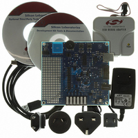
Manufacturer Part Number
C8051F336DK
Description
DEV KIT FOR C8051F336
Manufacturer
Silicon Laboratories Inc
Type
MCUr
Specifications of C8051F336DK
Contents
Evaluation Board, Power Supply, USB Cables, Adapter and Documentation
Processor To Be Evaluated
C8051F33x
Interface Type
USB, UART
Operating Supply Voltage
7 V to 15 V
Lead Free Status / RoHS Status
Lead free / RoHS Compliant
For Use With/related Products
C8051F336
Lead Free Status / Rohs Status
Lead free / RoHS Compliant
Other names
336-1430


C8051F336/7/8/9
26
Notes:
General
Solder Mask Design
Stencil Design
Card Assembly
Dimension
1. All dimensions shown are in millimeters (mm) unless otherwise noted.
2. This Land Pattern Design is based on the IPC-7351 guidelines.
3. All metal pads are to be non-solder mask defined (NSMD). Clearance between the solder
4. A stainless steel, laser-cut and electro-polished stencil with trapezoidal walls should be used
5. The stencil thickness should be 0.125mm (5 mils).
6. The ratio of stencil aperture to land pad size should be 1:1 for all perimeter pads.
7. A 2x2 array of 1.10mm x 1.10mm openings on a 1.30mm pitch should be used for the center
8. A No-Clean, Type-3 solder paste is recommended.
9. The recommended card reflow profile is per the JEDEC/IPC J-STD-020C specification for
C1
C2
X1
E
mask and the metal pad is to be 60μm minimum, all the way around the pad.
to assure good solder paste release.
pad.
Small Body Components.
Figure 5.2. QFN-24 Recommended PCB Land Pattern
Table 5.2. QFN-24 PCB Land Pattern Dimesions
3.90
3.90
0.20
Min
0.50 BSC
0.30
Max
4.00
4.00
Rev.1.0
Dimension
X2
Y1
Y2
2.70
0.65
2.70
Min
Max
2.80
0.75
2.80
Related parts for C8051F336DK
Image
Part Number
Description
Manufacturer
Datasheet
Request
R

Part Number:
Description:
SMD/C°/SINGLE-ENDED OUTPUT SILICON OSCILLATOR
Manufacturer:
Silicon Laboratories Inc
Part Number:
Description:
Manufacturer:
Silicon Laboratories Inc
Datasheet:
Part Number:
Description:
N/A N/A/SI4010 AES KEYFOB DEMO WITH LCD RX
Manufacturer:
Silicon Laboratories Inc
Datasheet:
Part Number:
Description:
N/A N/A/SI4010 SIMPLIFIED KEY FOB DEMO WITH LED RX
Manufacturer:
Silicon Laboratories Inc
Datasheet:
Part Number:
Description:
N/A/-40 TO 85 OC/EZLINK MODULE; F930/4432 HIGH BAND (REV E/B1)
Manufacturer:
Silicon Laboratories Inc
Part Number:
Description:
EZLink Module; F930/4432 Low Band (rev e/B1)
Manufacturer:
Silicon Laboratories Inc
Part Number:
Description:
I°/4460 10 DBM RADIO TEST CARD 434 MHZ
Manufacturer:
Silicon Laboratories Inc
Part Number:
Description:
I°/4461 14 DBM RADIO TEST CARD 868 MHZ
Manufacturer:
Silicon Laboratories Inc
Part Number:
Description:
I°/4463 20 DBM RFSWITCH RADIO TEST CARD 460 MHZ
Manufacturer:
Silicon Laboratories Inc
Part Number:
Description:
I°/4463 20 DBM RADIO TEST CARD 868 MHZ
Manufacturer:
Silicon Laboratories Inc
Part Number:
Description:
I°/4463 27 DBM RADIO TEST CARD 868 MHZ
Manufacturer:
Silicon Laboratories Inc
Part Number:
Description:
I°/4463 SKYWORKS 30 DBM RADIO TEST CARD 915 MHZ
Manufacturer:
Silicon Laboratories Inc
Part Number:
Description:
N/A N/A/-40 TO 85 OC/4463 RFMD 30 DBM RADIO TEST CARD 915 MHZ
Manufacturer:
Silicon Laboratories Inc
Part Number:
Description:
I°/4463 20 DBM RADIO TEST CARD 169 MHZ
Manufacturer:
Silicon Laboratories Inc