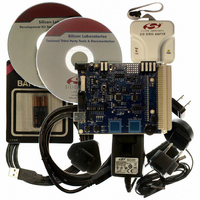
C8051F930DK Silicon Laboratories Inc, C8051F930DK Datasheet - Page 233

C8051F930DK
Manufacturer Part Number
C8051F930DK
Description
KIT DEV C8051F920,F921,F930,F931
Manufacturer
Silicon Laboratories Inc
Type
MCUr
Specifications of C8051F930DK
Contents
Target Board, Power Adapter, USB Debug Adapter, Cables, Batteries, and Software
Processor To Be Evaluated
C8051F930
Processor Series
C8051F9xx
Data Bus Width
8 bit
Interface Type
I2C, UART, SPI
Maximum Operating Temperature
+ 85 C
Minimum Operating Temperature
- 40 C
Operating Supply Voltage
0.9 V to 3.6 V
Lead Free Status / RoHS Status
Lead free / RoHS Compliant
For Use With/related Products
C8051F920, F921, F930, F931
Lead Free Status / Rohs Status
Lead free / RoHS Compliant
Other names
336-1473
Available stocks
Company
Part Number
Manufacturer
Quantity
Price
Company:
Part Number:
C8051F930DK
Manufacturer:
Silicon Labs
Quantity:
135
- Current page: 233 of 324
- Download datasheet (3Mb)
22. SMBus
The SMBus I/O interface is a two-wire, bi-directional serial bus. The SMBus is compliant with the System
Management Bus Specification, version 1.1, and compatible with the I
the interface by the system controller are byte oriented with the SMBus interface autonomously controlling
the serial transfer of the data. Data can be transferred at up to 1/20th of the system clock as a master or
slave (this can be faster than allowed by the SMBus specification, depending on the system clock used). A
method of extending the clock-low duration is available to accommodate devices with different speed
capabilities on the same bus.
The SMBus interface may operate as a master and/or slave, and may function on a bus with multiple
masters. The SMBus provides control of SDA (serial data), SCL (serial clock) generation and
synchronization, arbitration logic, and START/STOP control and generation. The SMBus peripheral can be
fully driven by software (i.e., software accepts/rejects slave addresses, and generates ACKs), or hardware
slave address recognition and automatic ACK generation can be enabled to minimize software overhead.
A block diagram of the SMBus peripheral and the associated SFRs is shown in Figure 22.1.
S
V
L
6
M
A
S
T
E
R
Interrupt
Request
S
V
L
5
M
O
D
T
X
E
SMB0ADR
S
V
L
4
SMB0CN
S
T
A
S
L
V
3
S
O
T
S
V
L
2
Q
A
C
K
R
S
L
V
1
A
R
B
O
S
L
T
S
V
L
0
C
A
K
G
C
S
I
S
V
M
L
6
Arbitration
SCL Synchronization
SCL Generation (Master Mode)
SDA Control
Hardware Slave Address Recognition
Hardware ACK Generation
IRQ Generation
M
SMBUS CONTROL LOGIC
S
L
V
5
SMB0ADM
M
S
V
L
4
M
S
L
V
3
M
S
V
L
2
M
E
N
S
B
Figure 22.1. SMBus Block Diagram
M
S
L
V
1
N
H
I
M
S
V
L
0
SMB0CF
B
U
S
Y
E
H
A
C
K
E
X
H
O
D
T
L
M
O
S
B
T
E
M
S
B
F
T
E
M
C
S
B
S
1
7
M
S
B
C
S
0
6
Data Path
SMB0DAT
5
Control
4
3
Rev. 1.1
2
1
0
00
01
10
11
Control
SDA
Control
SCL
C8051F93x-C8051F92x
T0 Overflow
T1 Overflow
TMR2H Overflow
TMR2L Overflow
FILTER
FILTER
2
N
N
C serial bus. Reads and writes to
SDA
SCL
C
R
O
S
S
B
A
R
Port I/O
233
Related parts for C8051F930DK
Image
Part Number
Description
Manufacturer
Datasheet
Request
R
Part Number:
Description:
SMD/C°/SINGLE-ENDED OUTPUT SILICON OSCILLATOR
Manufacturer:
Silicon Laboratories Inc
Part Number:
Description:
Manufacturer:
Silicon Laboratories Inc
Datasheet:
Part Number:
Description:
N/A N/A/SI4010 AES KEYFOB DEMO WITH LCD RX
Manufacturer:
Silicon Laboratories Inc
Datasheet:
Part Number:
Description:
N/A N/A/SI4010 SIMPLIFIED KEY FOB DEMO WITH LED RX
Manufacturer:
Silicon Laboratories Inc
Datasheet:
Part Number:
Description:
N/A/-40 TO 85 OC/EZLINK MODULE; F930/4432 HIGH BAND (REV E/B1)
Manufacturer:
Silicon Laboratories Inc
Part Number:
Description:
EZLink Module; F930/4432 Low Band (rev e/B1)
Manufacturer:
Silicon Laboratories Inc
Part Number:
Description:
I°/4460 10 DBM RADIO TEST CARD 434 MHZ
Manufacturer:
Silicon Laboratories Inc
Part Number:
Description:
I°/4461 14 DBM RADIO TEST CARD 868 MHZ
Manufacturer:
Silicon Laboratories Inc
Part Number:
Description:
I°/4463 20 DBM RFSWITCH RADIO TEST CARD 460 MHZ
Manufacturer:
Silicon Laboratories Inc
Part Number:
Description:
I°/4463 20 DBM RADIO TEST CARD 868 MHZ
Manufacturer:
Silicon Laboratories Inc
Part Number:
Description:
I°/4463 27 DBM RADIO TEST CARD 868 MHZ
Manufacturer:
Silicon Laboratories Inc
Part Number:
Description:
I°/4463 SKYWORKS 30 DBM RADIO TEST CARD 915 MHZ
Manufacturer:
Silicon Laboratories Inc
Part Number:
Description:
N/A N/A/-40 TO 85 OC/4463 RFMD 30 DBM RADIO TEST CARD 915 MHZ
Manufacturer:
Silicon Laboratories Inc
Part Number:
Description:
I°/4463 20 DBM RADIO TEST CARD 169 MHZ
Manufacturer:
Silicon Laboratories Inc


