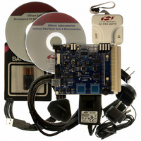
C8051F930DK Silicon Laboratories Inc, C8051F930DK Datasheet - Page 178

C8051F930DK
Manufacturer Part Number
C8051F930DK
Description
KIT DEV C8051F920,F921,F930,F931
Manufacturer
Silicon Laboratories Inc
Type
MCUr
Specifications of C8051F930DK
Contents
Target Board, Power Adapter, USB Debug Adapter, Cables, Batteries, and Software
Processor To Be Evaluated
C8051F930
Processor Series
C8051F9xx
Data Bus Width
8 bit
Interface Type
I2C, UART, SPI
Maximum Operating Temperature
+ 85 C
Minimum Operating Temperature
- 40 C
Operating Supply Voltage
0.9 V to 3.6 V
Lead Free Status / RoHS Status
Lead free / RoHS Compliant
For Use With/related Products
C8051F920, F921, F930, F931
Lead Free Status / Rohs Status
Lead free / RoHS Compliant
Other names
336-1473
Available stocks
Company
Part Number
Manufacturer
Quantity
Price
Company:
Part Number:
C8051F930DK
Manufacturer:
Silicon Labs
Quantity:
135
- Current page: 178 of 324
- Download datasheet (3Mb)
C8051F93x-C8051F92x
SFR Definition 16.2. DC0CF: DC-DC Converter Configuration
SFR Page = 0x0; SFR Address = 0x96
16.10. DC-DC Converter Specifications
See Table 4.14 on page 64 for a detailed listing of dc-dc converter specifications.
178
Reset
Name Reserved
Type
Bit
6:5 CLKDIV[1:0] DC
7
4
3
2
1
0
Bit
AD0CKINV ADC0 Clock Inversion (Clock Invert During Sync).
Reserved
VDDSLP
CLKSEL
CLKINV
ILIMIT
Name
R
7
0
Reserved.
Read = 0b; Must write 0b.
Divides the dc-dc converter clock when the system clock is selected as the clock
source for dc-dc converter. These bits are ignored when the dc-dc converter is
clocked from its local oscillator.
00: The dc-dc converter clock is system clock divided by 1.
01: The dc-dc converter clock is system clock divided by 2.
10: The dc-dc converter clock is system clock divided by 4.
11: The dc-dc converter clock is system clock divided by 8.
Inverts the ADC0 SAR clock derived from the dc-dc converter clock when the SYNC
bit (DC0CN.3) is enabled. This bit is ignored when the SYNC bit is set to zero.
0: ADC0 SAR clock is inverted.
1: ADC0 SAR clock is not inverted.
DC
Inverts the system clock used as the input to the dc-dc clock divider.
0: The dc-dc converter clock is not inverted.
1: The dc-dc converter clock is inverted.
Peak Current Limit Threshold.
Sets the threshold for the maximum allowed peak inductor current. See Table 16.1
for peak inductor current levels.
0: Peak inductor current is set at a lower level.
1: Peak inductor current is set at a higher level.
VDD
Specifies the power source for VDD/DC+ in Sleep Mode when the dc-dc converter is
enabled.
0: VDD-DC+ connected to VBAT in Sleep Mode.
1: VDD-DC+ is floating in Sleep Mode.
DC
Specifies the dc-dc converter clock source.
0: The dc-dc converter is clocked from its local oscillator.
1: The dc-dc converter is clocked from the system clock.
R/W
-
-
-
DC Clock Divider.
DC Converter Clock Invert.
DC Converter Clock Source Select.
0
-
6
CLKDIV[1:0]
DC+ Sleep Mode Connection.
R/W
5
0
AD0CKINV
Rev. 1.1
R/W
4
0
Function
CLKINV
R/W
3
0
ILIMIT
R/W
2
0
VDDSLP
R/W
1
0
CLKSEL
R/W
0
0
Related parts for C8051F930DK
Image
Part Number
Description
Manufacturer
Datasheet
Request
R
Part Number:
Description:
SMD/C°/SINGLE-ENDED OUTPUT SILICON OSCILLATOR
Manufacturer:
Silicon Laboratories Inc
Part Number:
Description:
Manufacturer:
Silicon Laboratories Inc
Datasheet:
Part Number:
Description:
N/A N/A/SI4010 AES KEYFOB DEMO WITH LCD RX
Manufacturer:
Silicon Laboratories Inc
Datasheet:
Part Number:
Description:
N/A N/A/SI4010 SIMPLIFIED KEY FOB DEMO WITH LED RX
Manufacturer:
Silicon Laboratories Inc
Datasheet:
Part Number:
Description:
N/A/-40 TO 85 OC/EZLINK MODULE; F930/4432 HIGH BAND (REV E/B1)
Manufacturer:
Silicon Laboratories Inc
Part Number:
Description:
EZLink Module; F930/4432 Low Band (rev e/B1)
Manufacturer:
Silicon Laboratories Inc
Part Number:
Description:
I°/4460 10 DBM RADIO TEST CARD 434 MHZ
Manufacturer:
Silicon Laboratories Inc
Part Number:
Description:
I°/4461 14 DBM RADIO TEST CARD 868 MHZ
Manufacturer:
Silicon Laboratories Inc
Part Number:
Description:
I°/4463 20 DBM RFSWITCH RADIO TEST CARD 460 MHZ
Manufacturer:
Silicon Laboratories Inc
Part Number:
Description:
I°/4463 20 DBM RADIO TEST CARD 868 MHZ
Manufacturer:
Silicon Laboratories Inc
Part Number:
Description:
I°/4463 27 DBM RADIO TEST CARD 868 MHZ
Manufacturer:
Silicon Laboratories Inc
Part Number:
Description:
I°/4463 SKYWORKS 30 DBM RADIO TEST CARD 915 MHZ
Manufacturer:
Silicon Laboratories Inc
Part Number:
Description:
N/A N/A/-40 TO 85 OC/4463 RFMD 30 DBM RADIO TEST CARD 915 MHZ
Manufacturer:
Silicon Laboratories Inc
Part Number:
Description:
I°/4463 20 DBM RADIO TEST CARD 169 MHZ
Manufacturer:
Silicon Laboratories Inc


