AT91SAM9M10-G45-EK Atmel, AT91SAM9M10-G45-EK Datasheet - Page 172
AT91SAM9M10-G45-EK
Manufacturer Part Number
AT91SAM9M10-G45-EK
Description
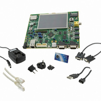
KIT EVAL FOR AT91SAMG45/9M10
Manufacturer
Atmel
Series
AT91SAM Smart ARMr
Type
MCUr
Specifications of AT91SAM9M10-G45-EK
Contents
Board, Cables, Power Supply
Processor To Be Evaluated
AT91SAM9M10
Processor Series
AT91SAM9
Data Bus Width
32 bit
Interface Type
RS-232, Ethernet, USB, JTAG
Operating Supply Voltage
5 V
Silicon Manufacturer
Atmel
Core Architecture
AVR
Kit Contents
Board
Features
Two High Speed USB Hosts, LCD TFT Display
Svhc
No SVHC (15-Dec-2010)
Mcu Supported Families
AT91SAM9M10,
Rohs Compliant
Yes
For Use With/related Products
AT91SAM9M10
Lead Free Status / RoHS Status
Lead free / RoHS Compliant
Available stocks
Company
Part Number
Manufacturer
Quantity
Price
Company:

Part Number:
AT91SAM9M10-G45-EK
Manufacturer:
INFINEON
Quantity:
10 000
Company:
Part Number:
AT91SAM9M10-G45-EK
Manufacturer:
Atmel
Quantity:
135


20.2.7.7
Figure 20-8. NAND Flash Application Example
172
External Bus Interface
NAND Flash Signals
AT91SAM9M10
NAND Flash Support
External Bus Interfaces integrate circuitry that interfaces to NAND Flash devices.
The NAND Flash logic is driven by the Static Memory Controller on the NCS3 address space.
Programming the EBI_CS3A field in the EBI_CSA Register in the Chip Configuration User Inter-
face to the appropriate value enables the NAND Flash logic. For details on this register, refer to
the Bus Matrix Section. Access to an external NAND Flash device is then made by accessing
the address space reserved to NCS3 (i.e., between 0x4000 0000 and 0x4FFF FFFF).
The NAND Flash Logic drives the read and write command signals of the SMC on the NANDOE
and NANDWE signals when the NCS3 signal is active. NANDOE and NANDWE are invalidated
as soon as the transfer address fails to lie in the NCS3 address space. See
172
section.
The address latch enable and command latch enable signals on the NAND Flash device are
driven by address bits A22 and A21 of the EBI address bus. The command, address or data
words on the data bus of the NAND Flash device are distinguished by using their address within
the NCSx address space. The chip enable (CE) signal of the device and the ready/busy (R/B)
signals are connected to PIO lines. The CE signal then remains asserted even when NCSx is
not selected, preventing the device from returning to standby mode.
EBI
for more information. For details on these waveforms, refer to the Static Memory Controller
PIO
PIO
NCSx/NANDCS
D[7:0]
A[22:21]
NANDWE
NANDOE
Not Connected
CE
R/B
ALE
CLE
NOE
NWE
AD[7:0]
NAND Flash
Figure 20-8 on page
6355B–ATARM–21-Jun-10
Related parts for AT91SAM9M10-G45-EK
Image
Part Number
Description
Manufacturer
Datasheet
Request
R

Part Number:
Description:
KIT EVAL FOR AT91SAM9M10
Manufacturer:
Atmel
Datasheet:

Part Number:
Description:
IC MCU 16/32BIT ARM9 324TFBGA
Manufacturer:
Atmel
Datasheet:

Part Number:
Description:
At91 Arm Thumb-based Microcontrollers
Manufacturer:
ATMEL Corporation
Datasheet:

Part Number:
Description:
MCU, MPU & DSP Development Tools KICKSTART KIT FOR AT91SAM9 PLUS
Manufacturer:
IAR Systems

Part Number:
Description:
DEV KIT FOR AVR/AVR32
Manufacturer:
Atmel
Datasheet:
Part Number:
Description:
INTERVAL AND WIPE/WASH WIPER CONTROL IC WITH DELAY
Manufacturer:
ATMEL Corporation
Datasheet:
Part Number:
Description:
Low-Voltage Voice-Switched IC for Hands-Free Operation
Manufacturer:
ATMEL Corporation
Datasheet:
Part Number:
Description:
MONOLITHIC INTEGRATED FEATUREPHONE CIRCUIT
Manufacturer:
ATMEL Corporation
Datasheet:
Part Number:
Description:
AM-FM Receiver IC U4255BM-M
Manufacturer:
ATMEL Corporation
Datasheet:
Part Number:
Description:
Monolithic Integrated Feature Phone Circuit
Manufacturer:
ATMEL Corporation
Datasheet:
Part Number:
Description:
Multistandard Video-IF and Quasi Parallel Sound Processing
Manufacturer:
ATMEL Corporation
Datasheet:
Part Number:
Description:
High-performance EE PLD
Manufacturer:
ATMEL Corporation
Datasheet: