MC56F8037EVM Freescale Semiconductor, MC56F8037EVM Datasheet - Page 28
MC56F8037EVM
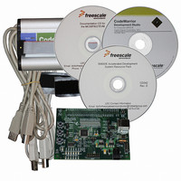
Manufacturer Part Number
MC56F8037EVM
Description
BOARD EVAL FOR MC56F8037
Manufacturer
Freescale Semiconductor
Type
MCUr
Datasheet
1.MC56F8037EVM.pdf
(180 pages)
Specifications of MC56F8037EVM
Contents
Board, Cables, CD, Debugger
Silicon Manufacturer
Freescale
Core Architecture
56800/E
Core Sub-architecture
56800/E
Silicon Core Number
MC56F
Silicon Family Name
MC56F80xx
Kit Contents
MC56F8037EVM, USB-JTAG Adapter, Cables, CD
Rohs Compliant
Yes
For Use With/related Products
MC56F8037
Lead Free Status / RoHS Status
Lead free / RoHS Compliant
Available stocks
Company
Part Number
Manufacturer
Quantity
Price
Company:

Part Number:
MC56F8037EVM
Manufacturer:
Freescale Semiconductor
Quantity:
135


28
Table 2-3 56F8037/56F8027 Signal and Package Information for the 64-Pin LQFP (Continued)
6
7
8
9
Return to
The TB2 signal is also brought out on the GPIOA13 pin.
The TB3 signal is also brought out on the GPIOA14 pin.
The TB1 signal is also brought out on the GPIOB11 pin.
The TA1 signal is also brought out on the GPIOB5 pin.
(CMPAI2)
(CMPBI2)
GPIOA10
GPIOA11
GPIOA12
(SCLK1)
Signal
(TB2
(TB3
(TB1
(TA1
Name
6
7
8
9
)
)
)
)
Table 2-2
Pin No.
LQFP
35
37
6
Output
Output
Output
Output
Output
Output
Output
Output
Input/
Input/
Input/
Input/
Input/
Input/
Input/
Input/
Type
Input
Input
State During
enabled
enabled
enabled
internal
internal
internal
pull-up
pull-up
pull-up
Reset
Input,
Input,
Input,
56F8037/56F8027 Data Sheet, Rev. 7
Port A GPIO — This GPIO pin can be individually programmed as
an input or output pin.
TB2 — Timer B, Channel 2.
Comparator A, Input 2 — This is an analog input to Comparator A.
After reset, the default state is GPIOA10. The peripheral functionality
is controlled via the SIM. See
Port A GPIO — This GPIO pin can be individually programmed as
an input or output pin.
TB3 — Timer B, Channel 3.
Comparator B, Input 2 — This is an analog input to Comparator B.
After reset, the default state is GPIOA11. The peripheral functionality
is controlled via the SIM. See
Port A GPIO — This GPIO pin can be individually programmed as
an input or output pin.
QSPI1 Serial Clock — In the master mode, this pin serves as an
output, clocking slaved listeners. In slave mode, this pin serves as
the data clock input. A Schmitt trigger input is used for noise
immunity.
TB1 — Timer B, Channel 1.
TA1 — Timer A, Channel 1.
After reset, the default state is GPIOA12. The peripheral functionality
is controlled via the SIM. See
Signal Description
Section
Section
Section
6.3.16.
6.3.16.
6.3.16.
Freescale Semiconductor
Related parts for MC56F8037EVM
Image
Part Number
Description
Manufacturer
Datasheet
Request
R

Part Number:
Description:
Manufacturer:
Freescale Semiconductor, Inc
Datasheet:
Part Number:
Description:
Manufacturer:
Freescale Semiconductor, Inc
Datasheet:
Part Number:
Description:
Manufacturer:
Freescale Semiconductor, Inc
Datasheet:
Part Number:
Description:
Manufacturer:
Freescale Semiconductor, Inc
Datasheet:
Part Number:
Description:
Manufacturer:
Freescale Semiconductor, Inc
Datasheet:
Part Number:
Description:
Manufacturer:
Freescale Semiconductor, Inc
Datasheet:
Part Number:
Description:
Manufacturer:
Freescale Semiconductor, Inc
Datasheet:
Part Number:
Description:
Manufacturer:
Freescale Semiconductor, Inc
Datasheet:
Part Number:
Description:
Manufacturer:
Freescale Semiconductor, Inc
Datasheet:
Part Number:
Description:
Manufacturer:
Freescale Semiconductor, Inc
Datasheet:
Part Number:
Description:
Manufacturer:
Freescale Semiconductor, Inc
Datasheet:
Part Number:
Description:
Manufacturer:
Freescale Semiconductor, Inc
Datasheet:
Part Number:
Description:
Manufacturer:
Freescale Semiconductor, Inc
Datasheet:
Part Number:
Description:
Manufacturer:
Freescale Semiconductor, Inc
Datasheet:
Part Number:
Description:
Manufacturer:
Freescale Semiconductor, Inc
Datasheet: