EVB9303 SMSC, EVB9303 Datasheet - Page 124
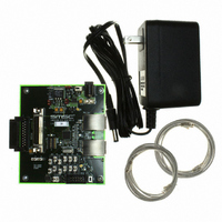
EVB9303
Manufacturer Part Number
EVB9303
Description
EVALUATION BOARD FOR LAN9303
Manufacturer
SMSC
Specifications of EVB9303
Main Purpose
Interface, Ethernet
Embedded
No
Utilized Ic / Part
LAN9303
Primary Attributes
3 Ports, 100BASE-TX/10BASE-T, Managed
Secondary Attributes
Full Duplex and HP Auto-MDIX Support, 10BASE-T and 100BASE-TX
Lead Free Status / Rohs Status
Lead free / RoHS Compliant
Other names
638-1095


WRITE
READ
Chapter 10 MII Management
Revision 1.4 (07-07-10)
10.1
10.2
PREAMBLE
32 1’s
32 1’s
This chapter details the MII management functionality provided by the device, which includes the
Slave
Controller
system CSRs. The
external PHY, dependant on the management mode. The PMI implements the IEEE 802.3
management protocol. The
and MII management path based on the selected mode of the device.
The SMI slave controller uses the same pins and protocol as the IEEE 802.3 MII management function,
and differs only in that SMI provides access to all internal registers by using a non-standard extended
addressing map. The SMI protocol co-exists with the MII management protocol by using the upper half
of the PHY address space (16 through 31). All direct and indirect registers can be accessed. The SMI
management mode is selected when the
management modes and their configuration settings are discussed in
Operation," on page
The MII management protocol is limited to 16-bit data accesses. The protocol is also limited to 5 PHY
address bits and 5 register address bits. The SMI frame format can be seen in
uses the PHY Address field bits 3:0 as the system register address bits 9:6, and the Register Address
field as the system register address bits 5:1. Therefore, Register Address field bit 0 is used as the
upper/lower word select. The device requires two back-to-back accesses to each register (with
alternate settings of Register Address field bit 0) which are combined to form a 32-bit access. The
access may be performed in any order.
Note: When accessing the device, the pair of cycles must be atomic. In this case, the first host SMI
Input data on the MDIO pin is sampled on the rising edge of the MDC input clock. Output data is
sourced on the MDIO pin with the rising edge of the clock. The MDIO pin is three-stated unless actively
driving read data.
A read or a write is performed using the frame format shown in
transferred msb first. Data bytes are transferred little endian. When Register Address bit 0 is 1, bytes
3 & 2 are selected with byte 3 occurring first. When Register Address bit 0 is 0, bytes 1 & 0 are
selected with byte 1 occurring first.
Functional Overview
SMI Slave Controller
Controller,
cycle is performed to the low/high word and the second host SMI cycle is performed to the
high/low word, forming a 32-bit transaction with no cycles to the device in between. With the
exception of Register Address field bit 0, all address and control bits must be the same for
both 16-bit cycles of a 32-bit transaction.
START
01
01
is used for CPU management of the device via the MII pins, and allows CPU access to all
CODE
PHY Management Interface
OP
10
01
PHY Management Interface (PMI)
19.
ADDRESS
MII Mode Multiplexer
Note 10.1
Table 10.1 SMI Frame Format
1AAAA
1AAAA
Small Form Factor Three Port 10/100 Managed Ethernet Switch with Single MII/RMII/Turbo MII
PHY
9876
9876
DATASHEET
REGISTER
ADDRESS
124
Note 10.1
AAAAA
AAAAA
54321
54321
mngt_mode_strap[1:0]
(PMI), and the
is used to direct the connections of the MII data path
is used to access the internal PHYs and optional
AROUND
Note 10.2
TURN-
TIME
Z0
10
MII Mode
Table
inputs are set to 01b. A list of
DDDDDDDDDDDDDDDD
DDDDDDDDDDDDDDDD
10.1. All addresses and data are
5432109876543210
5432109876543210
1111110000000000
1111110000000000
Multiplexer. The
Section 2.3, "Modes of
SMSC LAN9303/LAN9303i
Table
DATA
10.1. The device
SMI Slave
Datasheet
SMI
IDLE
Note
10.3
Z
Z
Related parts for EVB9303
Image
Part Number
Description
Manufacturer
Datasheet
Request
R


Part Number:
Description:
FAST ETHERNET PHYSICAL LAYER DEVICE
Manufacturer:
SMSC Corporation
Datasheet:
Part Number:
Description:
357-036-542-201 CARDEDGE 36POS DL .156 BLK LOPRO
Manufacturer:
SMSC Corporation
Datasheet:
Part Number:
Description:
357-036-542-201 CARDEDGE 36POS DL .156 BLK LOPRO
Manufacturer:
SMSC Corporation
Datasheet:
Part Number:
Description:
357-036-542-201 CARDEDGE 36POS DL .156 BLK LOPRO
Manufacturer:
SMSC Corporation
Datasheet:
Part Number:
Description:
4-PORT USB2.0 HUB CONTROLLER
Manufacturer:
SMSC Corporation
Datasheet:
Part Number:
Description:
Manufacturer:
SMSC Corporation
Datasheet:
Part Number:
Description:
Manufacturer:
SMSC Corporation
Datasheet:
Part Number:
Description:
FDC37C672ENHANCED SUPER I/O CONTROLLER WITH FAST IR
Manufacturer:
SMSC Corporation
Datasheet:
Part Number:
Description:
COM90C66LJPARCNET Controller/Transceiver with AT Interface and On-Chip RAM
Manufacturer:
SMSC Corporation
Datasheet:
Part Number:
Description:
Manufacturer:
SMSC Corporation
Datasheet:
Part Number:
Description:
Manufacturer:
SMSC Corporation
Datasheet:
Part Number:
Description:
Manufacturer:
SMSC Corporation
Datasheet:
Part Number:
Description:
Manufacturer:
SMSC Corporation
Datasheet: