EVL6563S-100W STMicroelectronics, EVL6563S-100W Datasheet - Page 22
EVL6563S-100W
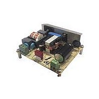
Manufacturer Part Number
EVL6563S-100W
Description
EVAL BOARD FOR L6563(100W)
Manufacturer
STMicroelectronics
Type
Power Factor Correctionr
Specifications of EVL6563S-100W
Main Purpose
Power Management, Power Factor Correction
Embedded
No
Utilized Ic / Part
L6563
Primary Attributes
100W Power Factor Correction and Preregulator Combination
Secondary Attributes
Transition Mode & Active Tracking Boost Function.
Board Size
90 mm x 83 mm
Maximum Operating Temperature
+ 60 C
Operating Supply Voltage
90 V to 265 V
Product
Power Management Modules
Dimensions
90 mm x 83 mm
Lead Free Status / RoHS Status
Lead free / RoHS Compliant
For Use With/related Products
L6563S
Other names
497-10490


Test results and significant waveforms
4.6
22/33
Figure 29. EVL6563S-100W TM PFC load
CH1: PFC output voltage
CH2: PFC_OK (pin #7)
CH3: gate drive (pin #13)
CH4: Iout
The event of an open loop is captured in
intervention, latching the operation of the L6563S. As mentioned previously, to restart the
system the input power must be recycled.
TBO (tracking boost option)
To use the TBO function on L6563S, a dedicated input of the multiplier is available on pin #6
(TBO). The function can be implemented by simply connecting a resistor (RT) between the
TBO pin and ground.
Usually, in traditional PFC stages, the DC output voltage is regulated at a fixed value
(typically 400 V) but in some applications, it may be advantageous to regulate the PFC
output voltage with the "tracking boost" or "follower boost" approach. In this way the circuit
with the TBO function provides better efficiency and thanks to the lower differential voltage
across the boost inductor, the value of L2 can be reduced as compared to the same circuit
without the TBO function.
The TBO pin presents a DC level equal to the peak of the MULT pin voltage and is
representative of the mains RMS voltage. The resistor defines a current, equal to
V(TBO)/RT, that is internally 1:1 mirrored and sunk from pin INV (pin 1) input of the error
amplifier. In this way, when the mains voltage increases, the voltage at the TBO pin
increases also as well as the current flowing through the resistor connected between TBO
and GND. Then a larger current will be sunk by the INV pin and the output voltage of the
PFC pre-regulator will be forced to go higher. Obviously, the output voltage will move in the
opposite direction if the input voltage decreases.
To avoid an undesired output voltage rise should the mains voltage exceed the maximum
specified value, the voltage at the TBO pin is clamped at 3 V. By properly selecting the
multiplier bias it is possible to set the maximum input voltage above which input-to-output
transient at 115 Vac, 60 Hz, full load
to no load
Doc ID 16279 Rev 2
Figure 30. EVL6563S-100W TM PFC open loop
CH1: PFC output voltage
CH2: Vcc (pin #14)
CH3: gate drive (pin #13)
CH4: PWM_LATCH (pin #8)
Figure
30. We can notice the protection
at 115 Vac, 60 Hz, full load
AN3065
Related parts for EVL6563S-100W
Image
Part Number
Description
Manufacturer
Datasheet
Request
R

Part Number:
Description:
EVAL BOARD FOR L6563(250W)
Manufacturer:
STMicroelectronics
Datasheet:

Part Number:
Description:
EVAL BOARD FOR L6563(400W)
Manufacturer:
STMicroelectronics
Datasheet:

Part Number:
Description:
Power Management Modules & Development Tools Tranisition Mode PFC L6563S EVL Board
Manufacturer:
STMicroelectronics
Datasheet:

Part Number:
Description:
EVAL BOARD L6563 (200W)
Manufacturer:
STMicroelectronics
Datasheet:
Part Number:
Description:
STMicroelectronics [RIPPLE-CARRY BINARY COUNTER/DIVIDERS]
Manufacturer:
STMicroelectronics
Datasheet:
Part Number:
Description:
STMicroelectronics [LIQUID-CRYSTAL DISPLAY DRIVERS]
Manufacturer:
STMicroelectronics
Datasheet:

Part Number:
Description:
BOARD EVAL FOR MEMS SENSORS
Manufacturer:
STMicroelectronics
Datasheet:
Part Number:
Description:
NPN TRANSISTOR POWER MODULE
Manufacturer:
STMicroelectronics
Datasheet:
Part Number:
Description:
TURBOSWITCH ULTRA-FAST HIGH VOLTAGE DIODE
Manufacturer:
STMicroelectronics
Datasheet:
Part Number:
Description:
Manufacturer:
STMicroelectronics
Datasheet:
Part Number:
Description:
DIODE / SCR MODULE
Manufacturer:
STMicroelectronics
Datasheet:
Part Number:
Description:
DIODE / SCR MODULE
Manufacturer:
STMicroelectronics
Datasheet: