EVL6563S-100W STMicroelectronics, EVL6563S-100W Datasheet - Page 13
EVL6563S-100W
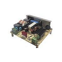
Manufacturer Part Number
EVL6563S-100W
Description
EVAL BOARD FOR L6563(100W)
Manufacturer
STMicroelectronics
Type
Power Factor Correctionr
Specifications of EVL6563S-100W
Main Purpose
Power Management, Power Factor Correction
Embedded
No
Utilized Ic / Part
L6563
Primary Attributes
100W Power Factor Correction and Preregulator Combination
Secondary Attributes
Transition Mode & Active Tracking Boost Function.
Board Size
90 mm x 83 mm
Maximum Operating Temperature
+ 60 C
Operating Supply Voltage
90 V to 265 V
Product
Power Management Modules
Dimensions
90 mm x 83 mm
Lead Free Status / RoHS Status
Lead free / RoHS Compliant
For Use With/related Products
L6563S
Other names
497-10490


AN3065
Figure 12. EVL6563H 100W TM PFC: Vds and
CH1: Q1 drain voltage
CH2: MULT voltage - Pin #3
CH4: L2 inductor current
is in phase with the input AC voltage, giving low distortion of the current waveform and high
power factor. On both the drain voltage traces, close to the zero-crossing points of the sine
wave, it is possible to note the action of the THD optimizer embedded in the L6563S. It is a
circuit that minimizes the conduction dead-angle of the AC input current near the zero-
crossings of the line voltage (crossover distortion). In this way, the THD (total harmonic
distortion) of the current is considerably reduced. A major cause of this distortion is the
inability of the system to transfer energy effectively when the instantaneous line voltage is
very low. This effect is magnified by the high-frequency filter capacitor placed after the
bridge rectifier, which retains some residual voltage that causes the diodes of the bridge
rectifier to be reverse-biased and the input current flow to temporarily stop. To overcome this
issue the device forces the PFC pre-regulator to process more energy near the line voltage
zero-crossings as compared to that commanded by the control loop. This results in both
minimizing the time interval where energy transfer is lacking and fully discharging the high-
frequency filter capacitor after the bridge. Essentially, the circuit artificially increases the ON-
time of the power switch with a positive offset added to the output of the multiplier in the
proximity of the line voltage zero-crossings. This offset is reduced as the instantaneous line
voltage increases, so that it becomes negligible as the line voltage moves toward the top of
the sinusoid. Furthermore the offset is modulated by the voltage on the V
have little offset at low line, where energy transfer at zero-crossings is typically quite good,
and a larger offset at high line where the energy transfer gets worse.
To obtain maximum benefit from the THD optimizer circuit, the high-frequency filter
capacitors after the bridge rectifier should be minimized, compatibly with EMI filtering needs.
A large capacitance, in fact, introduces a conduction dead-angle of the AC input current in
itself, thus reducing the effectiveness of the optimizer circuit.
In
operating frequency and the current peak at top of the input sine wave during operation at
100 Vac and 230 Vac. The multiplier waveform has been captured as a reference.
inductor current at 100 Vac, 50 Hz,
full load
Figure 13
and
15
the detail of the waveforms at switching frequency allows measuring the
Doc ID 16279 Rev 2
Figure 13. EVL6563H 100W TM PFC: Vds and
CH4: Q1 drain voltage
CH2: MULT voltage - pin #3
CH1: L2 inductor current
Test results and significant waveforms
inductor current at 100 Vac, 50 Hz,
full load (detail)
FF
pin so as to
13/33
Related parts for EVL6563S-100W
Image
Part Number
Description
Manufacturer
Datasheet
Request
R

Part Number:
Description:
EVAL BOARD FOR L6563(250W)
Manufacturer:
STMicroelectronics
Datasheet:

Part Number:
Description:
EVAL BOARD FOR L6563(400W)
Manufacturer:
STMicroelectronics
Datasheet:

Part Number:
Description:
Power Management Modules & Development Tools Tranisition Mode PFC L6563S EVL Board
Manufacturer:
STMicroelectronics
Datasheet:

Part Number:
Description:
EVAL BOARD L6563 (200W)
Manufacturer:
STMicroelectronics
Datasheet:
Part Number:
Description:
STMicroelectronics [RIPPLE-CARRY BINARY COUNTER/DIVIDERS]
Manufacturer:
STMicroelectronics
Datasheet:
Part Number:
Description:
STMicroelectronics [LIQUID-CRYSTAL DISPLAY DRIVERS]
Manufacturer:
STMicroelectronics
Datasheet:

Part Number:
Description:
BOARD EVAL FOR MEMS SENSORS
Manufacturer:
STMicroelectronics
Datasheet:
Part Number:
Description:
NPN TRANSISTOR POWER MODULE
Manufacturer:
STMicroelectronics
Datasheet:
Part Number:
Description:
TURBOSWITCH ULTRA-FAST HIGH VOLTAGE DIODE
Manufacturer:
STMicroelectronics
Datasheet:
Part Number:
Description:
Manufacturer:
STMicroelectronics
Datasheet:
Part Number:
Description:
DIODE / SCR MODULE
Manufacturer:
STMicroelectronics
Datasheet:
Part Number:
Description:
DIODE / SCR MODULE
Manufacturer:
STMicroelectronics
Datasheet: