MCP1631RD-MCC2 Microchip Technology, MCP1631RD-MCC2 Datasheet - Page 6
MCP1631RD-MCC2
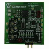
Manufacturer Part Number
MCP1631RD-MCC2
Description
REFERENCE DESIGN MCP1631HV
Manufacturer
Microchip Technology
Datasheets
1.MCP1631VHVT-330EST.pdf
(34 pages)
2.MCP1631HV-330EST.pdf
(54 pages)
3.MCP1631RD-MCC2.pdf
(20 pages)
4.MCP1631RD-MCC2.pdf
(328 pages)
Specifications of MCP1631RD-MCC2
Main Purpose
Power Management, Battery Charger
Embedded
Yes, MCU, 8-Bit
Utilized Ic / Part
MCP1631HV, PIC16F883
Primary Attributes
1 ~ 2 Cell- Li-Ion, 1 ~ 5 Cell- NiCd/NiMH, 1 ~ 2 1W LEDs
Secondary Attributes
Status LEDs
Silicon Manufacturer
Microchip
Application Sub Type
Battery Charger
Kit Application Type
Power Management - Battery
Silicon Core Number
MCP1631HV, PIC16F883
Kit Contents
Board
Lead Free Status / RoHS Status
Lead free / RoHS Compliant
Lead Free Status / RoHS Status
Lead free / RoHS Compliant


AN1137
HIGH SPEED ANALOG PWM OPERATION
The high-speed analog PWM is used to control the
power train switch ON and OFF times to regulate the
output of the converter. Voltage or current can be
regulated depending on what is being sensed. For the
SEPIC Battery Charger application, the MCP1631HV
is always regulating current, the microcontroller is
programming this current.
The analog PWM starts with the oscillator input,
typically a microcontroller PWM output or simple clock
output (50% duty cycle). When the oscillator input is
high, the V
FET Driver is ON). A new cycle is started when the
OSC_IN input transitions from a high to a low, the inter-
nal N-channel MOSFET driver turns off and the P-
Channel MOSFET turns on driving the V
turning on the external N-Channel MOSFET. Current
begins to ramp up in the external CS sense resistor
until it reaches 1/3 of the level of the error amplifier
output voltage (limited to 0.9V by error amplifier clamp).
The 0.9V limit is used as an overcurrent limit, the
FIGURE 5:
DS01137A-page 6
Note 1: A1 output or COMP is clamped to 2.7V maximum to set current limit.
V
V
CS INPUT
OSC_IN
Low = Active Duty Cycle
High = V
FB
REF
EXT
output is pulled low, (N-Channel MOS-
V = COMP/3
EXT
Error Amplifier
and Compensation
+
-
A1
Analog PWM Operation.
OFF
COMP
2R
R
EXT
+
-
pin high
High Speed Comparator
C1
S
R
Latch
ramping current is used for peak current mode control
CS signal. A filter is used on the CS input to remove the
leading edge turn on spike associated with the turn on
of the external power MOSFET. The driver P-Channel
MOSFET is powered using a separate P
helping to keep switching noise off of the A
sensitive CS circuitry.
The error amplifier is configured as an integrator, so
any difference between its inputs, V
quickly removed. If the V
error amplifiers output, (COMP), will be pulled down,
lowering the peak current into the switch and lowering
duty cycle bringing the output back into regulation. The
external R and C used for compensation is used to con-
trol the speed of the error amplifiers output response. If
not compensated properly, the error amplifier output
will move to fast (unstable system with under damped
oscillations) or slow (over damped system with no
performance or response to changes). The V
is set by the microcontroller to program the proper
charge current.
Q
© 2007 Microchip Technology Inc.
FB
input is high, the inverting
P
P
VDD
GND
MOSFET P
MOSFET N
V
REF
EXT
and V
VDD
REF
VDD
pin and
FB
input
are
pin
Related parts for MCP1631RD-MCC2
Image
Part Number
Description
Manufacturer
Datasheet
Request
R

Part Number:
Description:
REFERENCE DESIGN FOR MCP1631HV
Manufacturer:
Microchip Technology
Datasheet:

Part Number:
Description:
REF DES BATT CHARG OR LED DRIVER
Manufacturer:
Microchip Technology
Datasheet:

Part Number:
Description:
Manufacturer:
Microchip Technology Inc.
Datasheet:
Part Number:
Description:
Manufacturer:
Microchip Technology Inc.
Datasheet:
Part Number:
Description:
Manufacturer:
Microchip Technology Inc.
Datasheet:
Part Number:
Description:
Manufacturer:
Microchip Technology Inc.
Datasheet:
Part Number:
Description:
Manufacturer:
Microchip Technology Inc.
Datasheet:
Part Number:
Description:
Manufacturer:
Microchip Technology Inc.
Datasheet:
Part Number:
Description:
Manufacturer:
Microchip Technology Inc.
Datasheet:
Part Number:
Description:
Manufacturer:
Microchip Technology Inc.
Datasheet: