MCP1631RD-MCC2 Microchip Technology, MCP1631RD-MCC2 Datasheet - Page 17
MCP1631RD-MCC2
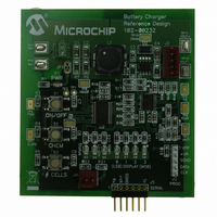
Manufacturer Part Number
MCP1631RD-MCC2
Description
REFERENCE DESIGN MCP1631HV
Manufacturer
Microchip Technology
Datasheets
1.MCP1631VHVT-330EST.pdf
(34 pages)
2.MCP1631HV-330EST.pdf
(54 pages)
3.MCP1631RD-MCC2.pdf
(20 pages)
4.MCP1631RD-MCC2.pdf
(328 pages)
Specifications of MCP1631RD-MCC2
Main Purpose
Power Management, Battery Charger
Embedded
Yes, MCU, 8-Bit
Utilized Ic / Part
MCP1631HV, PIC16F883
Primary Attributes
1 ~ 2 Cell- Li-Ion, 1 ~ 5 Cell- NiCd/NiMH, 1 ~ 2 1W LEDs
Secondary Attributes
Status LEDs
Silicon Manufacturer
Microchip
Application Sub Type
Battery Charger
Kit Application Type
Power Management - Battery
Silicon Core Number
MCP1631HV, PIC16F883
Kit Contents
Board
Lead Free Status / RoHS Status
Lead free / RoHS Compliant
Lead Free Status / RoHS Status
Lead free / RoHS Compliant


The peak switch voltage is equal to V
SEPIC converter. Any leakage inductance voltage
spike is clamped through the output diode by the output
capacitor. A switch voltage rating for this application
should be a minimum of V
A 30V, 30 milli-ohm, logic-level switch is selected.
MOSFET switching losses should also be considered
when selecting the MOSFET switch. Low on resistance
switches tend to have high capacitance and will switch
slower, increasing switching losses. The lowest R
MOSFET is not necessarily the best choice. When
using the SOIC-8 package for a 30V MOSFET, there
are many choices available.
SEPIC Diode Voltage and Current Calculations
A schottky diode is recommended for low-voltage
applications. For battery charger applications, the
SEPIC diode will block current flow from the battery
back to the input. The reverse leakage current of the
selected schottky diode can be a critical parameter, if
low battery drain is desired. Low schottky diode forward
drop is also a key parameter; the low drop improves
converter efficiency.
The maximum reverse voltage across the SEPIC diode
occurs during the switch on time. The cathode of the
schottky diode is connected to V
schottky diode is connected to the SEPIC coupling
capacitor. The voltage across the coupling capacitor
voltage is equal to V
equal to V
The peak SEPIC diode current occurs when the switch
is turned off. The peak diode current is equal to the
peak current in W
3.14A. The average diode current is equal to the output
current (I
diode in the path of the output.
SEPIC Coupling Capacitor (C
Calculations and Voltage Rating
The RMS current in the SEPIC coupling capacitor is
mainly dependant upon output power with some
influence by inductor ripple current. As output power
increases, the capacitor ripple current will increase as
well. As shown in
the current in winding 2 (output current) is flowing
through the coupling capacitor C
time, the C
number 1 (W
current is equal to the average input current. Therefore,
the worst case or maximum RMS current in the
coupling capacitor will occur at maximum output power
© 2007 Microchip Technology Inc.
V
V
SW
SW
OUT
= 12V +4.2V
= 16.2V
OUT
1
current is equal to the current in winding
), typical of all topologies with a series
- (-V
1
). As previously discussed, the W
Figure 12
IN
2
, plus the peak current in W
IN
) or V
; the voltage across the diode is
IN
OUT
(during the switch on time),
(MAX) + V
+ V
1
OUT
1
. During the switch off
) RMS Current
IN
.
, the anode of the
IN
OUT
+ V
(MAX).
OUT
for the
DSON
1
or
1
and minimum input voltage. To estimate size for the
coupling capacitor, the capacitor derivative equation
can be used.
The rate of change of voltage across the capacitor is
related to the amount of current through the capacitor
and the size or energy storage capability of the
capacitor.
For the SEPIC converter coupling capacitor, the
voltage is approximated to be a DC value when
deriving the duty cycle. The ripple voltage should be no
more than 5% of the voltage across the capacitor or the
input voltage. In this example, the input voltage and C
DC voltage is 12V, so there should be no more than 5%
or 600 mV of ripple on the coupling capacitor.
In this example there is an average of 2A flowing
through the coupling capacitor during the switch on
time. The on time is approximately 26% or 520 ns. To
keep the capacitor voltage ripple less than 5% of V
or 600 mV, the amount of capacitance is equal to (2A)
/ (600mV/520 ns) or 1.73 µF. For this application a
standard value 2.2 µF X7R 25V rated ceramic
capacitor should be used.
FIGURE 13:
As shown in
current is largely dependent upon output power and
input voltage. As the input voltage decreases, the
current in W
current flowing in W
C
changes magnitude and direction so that the current
flowing in C
and direction.
1
. When the switch turns off, the current quickly
Note:
I
I
W2
W1
0
1
1
Area above 0 equals the area below
zero.
is equal to the current in W
increases. During the switch on time, the
Figure
- I
I
W1
2
C
13, the coupling capacitor ripple
is equal to the current flowing in
=
C
1
C
+ I
Ripple Current.
×
W2
dV
------ -
dt
AN1137
DS01137A-page 17
1
, magnitude
I
C1
IN
1
,
Related parts for MCP1631RD-MCC2
Image
Part Number
Description
Manufacturer
Datasheet
Request
R

Part Number:
Description:
REFERENCE DESIGN FOR MCP1631HV
Manufacturer:
Microchip Technology
Datasheet:

Part Number:
Description:
REF DES BATT CHARG OR LED DRIVER
Manufacturer:
Microchip Technology
Datasheet:

Part Number:
Description:
Manufacturer:
Microchip Technology Inc.
Datasheet:
Part Number:
Description:
Manufacturer:
Microchip Technology Inc.
Datasheet:
Part Number:
Description:
Manufacturer:
Microchip Technology Inc.
Datasheet:
Part Number:
Description:
Manufacturer:
Microchip Technology Inc.
Datasheet:
Part Number:
Description:
Manufacturer:
Microchip Technology Inc.
Datasheet:
Part Number:
Description:
Manufacturer:
Microchip Technology Inc.
Datasheet:
Part Number:
Description:
Manufacturer:
Microchip Technology Inc.
Datasheet:
Part Number:
Description:
Manufacturer:
Microchip Technology Inc.
Datasheet: