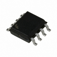
FAN6520AIMX Fairchild Semiconductor, FAN6520AIMX Datasheet - Page 7

FAN6520AIMX
Manufacturer Part Number
FAN6520AIMX
Description
IC CTRLR PWM SGL SYNC BUCK 8SOIC
Manufacturer
Fairchild Semiconductor
Type
Step-Down (Buck)r
Datasheet
1.FAN6520AMX.pdf
(15 pages)
Specifications of FAN6520AIMX
Internal Switch(s)
No
Synchronous Rectifier
Yes
Number Of Outputs
1
Voltage - Output
0.8 ~ 5.5 V
Frequency - Switching
300kHz
Voltage - Input
4.5 ~ 5.5 V
Operating Temperature
-40°C ~ 85°C
Mounting Type
Surface Mount
Package / Case
8-SOIC (3.9mm Width)
Power - Output
715mW
Topology
Boost, Buck
Output Voltage
0.8 V to 5.5 V
Switching Frequency
340 KHz
Duty Cycle (max)
100 %
Operating Supply Voltage
5 V
Maximum Operating Temperature
+ 85 C
Minimum Operating Temperature
- 40 C
Mounting Style
SMD/SMT
Synchronous Pin
No
Lead Free Status / RoHS Status
Lead free / RoHS Compliant
Current - Output
-
Lead Free Status / Rohs Status
Lead free / RoHS Compliant
©2005 Fairchild Semiconductor Corporation
FAN6520A Rev. 1.0.5
The FAN6520A incorporates a MOSFET shoot-through
protection method that allows a converter to both sink
and source current. Care should be exercised when
designing a converter with the FAN6520A when it is
known that the converter may sink current.
When the converter is sinking current, it is behaving as a
boost converter regulating its input voltage. This means
that the converter is boosting current into the V
which supplies the bias voltage to the FAN6520A. If this
current has nowhere to go—such as to other distributed
loads on the V
tion device, or other methods—the capacitance on the
V
level of the V
rail is boosted to a level that exceeds the maximum volt-
age rating of the FAN6520A, the IC experiences an irre-
versible failure and the converter is no longer
operational. Ensure that there is a path for the current to
follow, other than the capacitance on the rail, to prevent
this failure mode.
Application Information
Layout Considerations
In any high-frequency switching converter, layout is very
important. Switching current from one power device to
another can generate voltage transients across the
impedances of the interconnecting bond wires and circuit
traces. Use wide, short-printed traces to minimize inter-
connecting impedances. The critical components should
be located as close together as possible, using ground
plane construction or single-point grounding.
CC
bus absorbs the current. This allows the voltage
CC
Figure 4. Soft-Start Interval
CC
rail to increase. If the voltage level of the
rail, through a voltage limiting protec-
CC
rail,
Figure 5 shows the critical power components of the con-
verter. To minimize voltage overshoot, the interconnect-
ing wires (indicated by heavy lines) should be part of a
ground or power plane in a printed circuit board. The
components shown in Figure 5 should be located as
close together as possible. Note that the capacitors C
and C
itors. Locate the FAN6520A within two inches of the Q1
and Q2 MOSFETs. The circuit traces for the MOSFETs’
gate and source connections from the FAN6520A must
be sized to handle up to 1A peak current.
Figure 5 shows the circuit traces that require additional
layout consideration. Use single point and ground plane
construction for the circuits shown. Minimize any leakage
current paths on the COMP/OCSET pin and locate the
resistor, R
because the internal current source is only 20µA. Pro-
vide local V
pins. Locate the capacitor, CBOOT, as close as practical
to the BOOT and PHASE pins. All components used for
feedback compensation should be located as close to
the IC as practical.
+5V
7
Figure 6. PCB Small Signal Layout Guidelines
OUT
Figure 5. Printed Circuit Board Power and
HDRV
SW
LDRV
COMP/OCSET
FAN6520A
may each represent numerous physical capac-
OSCET,
CC
Ground Planes or Islands
Q1
Q2
decoupling between the VCC and GND
close to the COMP/OCSET pin
D
BOOT
SW
VCC
GND
BOOT
Vin
L
OUT
C
VCC
C
+5V
BOOT
Vin
Q1
Q2
C
www.fairchildsemi.com
C
IN
L
C
OUT
OUT
OUT
+V
OUT
+V
OUT
IN


