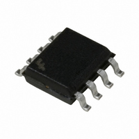
FAN6520AIMX Fairchild Semiconductor, FAN6520AIMX Datasheet - Page 11

FAN6520AIMX
Manufacturer Part Number
FAN6520AIMX
Description
IC CTRLR PWM SGL SYNC BUCK 8SOIC
Manufacturer
Fairchild Semiconductor
Type
Step-Down (Buck)r
Datasheet
1.FAN6520AMX.pdf
(15 pages)
Specifications of FAN6520AIMX
Internal Switch(s)
No
Synchronous Rectifier
Yes
Number Of Outputs
1
Voltage - Output
0.8 ~ 5.5 V
Frequency - Switching
300kHz
Voltage - Input
4.5 ~ 5.5 V
Operating Temperature
-40°C ~ 85°C
Mounting Type
Surface Mount
Package / Case
8-SOIC (3.9mm Width)
Power - Output
715mW
Topology
Boost, Buck
Output Voltage
0.8 V to 5.5 V
Switching Frequency
340 KHz
Duty Cycle (max)
100 %
Operating Supply Voltage
5 V
Maximum Operating Temperature
+ 85 C
Minimum Operating Temperature
- 40 C
Mounting Style
SMD/SMT
Synchronous Pin
No
Lead Free Status / RoHS Status
Lead free / RoHS Compliant
Current - Output
-
Lead Free Status / Rohs Status
Lead free / RoHS Compliant
©2005 Fairchild Semiconductor Corporation
FAN6520A Rev. 1.0.5
High-Side Losses
Figure 10 shows a MOSFET’s switching interval, with the
upper graph being the voltage and current on the drain-
to-source and the lower graph detailing V
a constant current charging the gate. The x-axis, there-
fore, is also representative of gate charge (Q
C
receives the current from the gate driver during t3 (as
V
lower graph are either specified or can be derived from
the MOSFET’s datasheet.
Assuming switching losses are about the same for both
the rising edge and falling edge, Q1’s switching losses
occur during the shaded time when the MOSFET has
voltage across it and current through it.
These losses are given by:
P
where P
and P
given MOSFET, R
perature (T
time) and is t2+t3 (Figure 10).
The driver’s impedance and C
period is controlled by the driver’s impedance and Q
Since most of t
current assumption for the driver to simplify the calcula-
tion of t
P COND
P SW
t s
DS
UPPER
GD
≈
is falling). The gate charge (Q
+ C
------------------------- -
I DRIVER
Q G SW
COND
=
S
= P
UPPER
:
GS
(
⎛
⎝
=
V DS I L
----------------------- -
J
are the switching and conduction losses for a
SW
), and t
⎛
⎜
⎝
and it controls t1, t2, and t4 timing. C
V OUT
---------------- -
)
2
V IN
S
is the upper MOSFET’s total losses, P
+ P
≈
×
occurs when V
-------------------------------------------------------------- -
⎛
⎜
⎝
DS(ON)
COND
-------------------------------------------------------- -
R DRIVER
S
⎞
⎟
⎠
×
is the switching period (rise or fall
×
2
I OUT
V
×
is at the maximum junction tem-
Q G SW
CC
t s
⎞ F
⎠
2
(
–
×
ISS
+
SW
V SP
GS
R DS ON
R GATE
determine t2, while t3’s
)
= V
G
) parameters on the
(
SP,
⎞
⎟
⎠
GS
)
use a constant
vs. time with
G
). C
ISS
(27)
(25)
(24)
(26)
GD
SW
GD
=
.
Most MOSFET vendors specify Q
can be determined as Q
Q
threshold (V
which can be as high as 20V in a typical portable appli-
cation. Care should be taken to include the delivery of
the MOSFET’s gate power (P
power dissipation required:
P
where Q
GATE
TH
11
V
V
V
DS
V
is the gate charge required to reach the MOSFET
I
TH
GS
D
SP
= Q
G
Figure 10. Switching Losses and Q
Figure 11. Drive Equivalent Circuit
5V
is the total gate charge to reach V
G
R
TH
× V
D
t1
). For the high-side MOSFET, V
C
CC
Q
ISS
GS
× F
t2
SW
G(SW)
SW
HDRV
Q
G(SW)
C
= Q
Q
GD
GATE
GD
t3
G
GD
GD
) in calculating the
+ Q
R
and Q
GATE
C
GS
C
GS
t4
GD
C
www.fairchildsemi.com
– Q
GS
CC
ISS
G
. Q
.
DS
TH
V
t5
IN
4.5V
where
= V
G(SW)
(28)
IN
,


