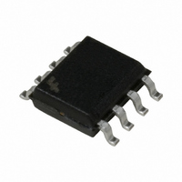
FAN6520AIMX Fairchild Semiconductor, FAN6520AIMX Datasheet

FAN6520AIMX
Specifications of FAN6520AIMX
Related parts for FAN6520AIMX
FAN6520AIMX Summary of contents
Page 1
... Low-Voltage Distributed Power Supplies Ordering Information Part Number FAN6520AM FAN6520AMX FAN6520AIM FAN6520AIMX © 2005 Fairchild Semiconductor Corporation FAN6520A Rev. 1.0.5 Description The FAN6520A simplifies implementing a complete con- trol and protection scheme for a DC-DC stepdown con- verter. Designed to drive N-channel MOSFETs in a ...
Page 2
... SW Switch Node Input. The SW pin provides return for the high-side bootstrapped driver sense point for the adaptive shoot-through protection, and is used to monitor the drop across the upper MOSFET’s R © 2005 Fairchild Semiconductor Corporation FAN6520A Rev. 1.0.5 BOOT ...
Page 3
... Typical Application +5V R OCSET COMP/OCSET VCC SAMPLE & HOLD COMP/OCSET FB ERROR AMP 0.8V © 2005 Fairchild Semiconductor Corporation FAN6520A Rev. 1.0.5 BOOT 1 VCC Q1 5 HDRV C 2 VCC SW FAN6520A 8 Q2 LDRV 4 GND Figure 1. Typical Application POR / SOFT-START OC PWM PWM 20A OSC Figure 2. Functional Block Diagram ...
Page 4
... Thermal Resistance, Junction-to-Case JC Θ Thermal Resistance, Junction-to-Ambient JA Recommended Operating Conditions Symbol Parameter V Supply Voltage CC T Ambient Temperature A T Junction Temperature J © 2005 Fairchild Semiconductor Corporation FAN6520A Rev. 1.0.5 Min. –0.5 –0.5 –3 = 25°C A Conditions Min. VCC to PGND 4.5 FAN6520A 0 FAN6520AI –40 –40 4 Max ...
Page 5
... OCSET V Disable Threshold DISABLE Notes: 1. All limits at operating temperature extremes are guaranteed by design, characterization, and statistical quality control specifications guaranteed by design/characterization (not production tested). © 2005 Fairchild Semiconductor Corporation FAN6520A Rev. 1.0.5 Conditions Min. HDRV, LDRV open • 1.5 • 4.00 FAN6520A • ...
Page 6
... The converter dissipates very little power with this method. The measured input power for the conditions shown in Figure 3 is 1.5W. OUTPUT INDUCTOR CURRENT 5A/DIV. Figure 3. Over-Current Operation ©2005 Fairchild Semiconductor Corporation FAN6520A Rev. 1.0.5 The over-current function trips at a peak inductor current (I ) determined by: PEAK I ...
Page 7
... Use wide, short-printed traces to minimize inter- connecting impedances. The critical components should be located as close together as possible, using ground plane construction or single-point grounding. ©2005 Fairchild Semiconductor Corporation FAN6520A Rev. 1.0.5 Q1 HDRV SW Q2 LDRV Figure 5 ...
Page 8
... ------------------------------------ × × ESR 2π ESR C ©2005 Fairchild Semiconductor Corporation FAN6520A Rev. 1.0.5 The compensation network consists of the error amplifier (internal to the FAN6520A) and the impedance networks Z and compared provide a closed-loop transfer function with the highest E/A 0dB crossing frequency (F gin. Phase margin is the difference between the closed- loop phase at F below relate the compensation network’ ...
Page 9
... Generally, multiple small-case electrolytic capaci- tors perform better than a single large-case capacitor. ©2005 Fairchild Semiconductor Corporation FAN6520A Rev. 1.0.5 Output Inductor (L The output inductor is selected to meet the output volt- ...
Page 10
... GS(Q1) SW where Q is total gate charge of Q1 for its applied V G1 ©2005 Fairchild Semiconductor Corporation FAN6520A Rev. 1.0.5 As described in the equations above, the total power consumed in driving the gate is divided in proportion to the resistances in series with the MOSFET's internal ) for the input RMS gate node, as shown in Figure 9 ...
Page 11
... Q Since most of t occurs when current assumption for the driver to simplify the calcula- tion ≈ ≈ ------------------------- - -------------------------------------------------------------- - DRIVER ⎛ – CC ⎜ -------------------------------------------------------- - ⎝ R DRIVER + ©2005 Fairchild Semiconductor Corporation FAN6520A Rev. 1.0 vs. time with ISS GD ) parameters on the (24) GS (25 (26) SW determine t2, while t3’s . ...
Page 12
... Since D MIN duces a conservative result, simplifying the calculation. The maximum power dissipation (P of the maximum allowable die temperature of the low- ©2005 Fairchild Semiconductor Corporation FAN6520A Rev. 1.0.5 side MOSFET, the θ ambient temperature rise: Ý 0.5V. Since P is ...
Page 13
... Not Populated R4 2.49kΩ Resistor, 603 R5 11.8kΩ Resistor, 603 R6 Not Populated Resistor, 603 R7 0Ω Resistor, 603 PB1 Pushbutton, miniature U1 Single Synchronous Buck PWM TP1,2,3,4 Test Points © 2005 Fairchild Semiconductor Corporation FAN6520A Rev. 1.0.5 BOOT HDRV FAN6520A Q2 LDRV 4 GND ...
Page 14
... Dimensional Outline Drawing © 2005 Fairchild Semiconductor Corporation FAN6520A Rev. 1.0.5 Figure 13. 8-Lead SOIC Package Drawing 14 www.fairchildsemi.com ...
Page 15
... Fairchild Semiconductor Corporation FAN6520A Rev. 1.0.5 15 www.fairchildsemi.com ...


