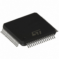
L6713A STMicroelectronics, L6713A Datasheet - Page 8

L6713A
Manufacturer Part Number
L6713A
Description
IC CTRLR 2/3PH W/DRIVERS 64-TQFP
Manufacturer
STMicroelectronics
Datasheet
1.L6713ATR.pdf
(64 pages)
Specifications of L6713A
Applications
Controller, Intel VR10, VR11, AMD CPU
Voltage - Input
12V
Number Of Outputs
3
Voltage - Output
0.3 ~ 1.6 V
Operating Temperature
0°C ~ 70°C
Mounting Type
Surface Mount
Package / Case
64-TQFP Exposed Pad, 64-eTQFP, 64-HTQFP, 64-VQFP
Output Current
2 A
Mounting Style
SMD/SMT
Maximum Operating Temperature
+ 125 C
Minimum Operating Temperature
0 C
Lead Free Status / RoHS Status
Lead free / RoHS Compliant
Available stocks
Company
Part Number
Manufacturer
Quantity
Price
Pin settings
8/64
Table 2.
N°
17
18
19
20
21
22
23
24
25
26
27
28
29
DROOP
OUTEN
COMP
SGND
VSEN
CS2+
CS3+
CS2-
CS3-
N.C.
N.C.
LTB
Pin
FB
Pin description (continued)
Not internally connected.
Not internally connected.
Output enable pin. Internally pulled up by 12.5 µA(typ) to 5 V.
Forced low, the device stops operations with all MOSFETs OFF: all the
protections are disabled except for
Leave floating, the device starts-up implementing soft-start up to the selected
VID code.
Cycle this pin to recover latch from protections; filter with 1 nF (typ) vs. SGND.
Load transient boost pin.
Internally fixed at 1 V, connecting a R
Load transient boost technology
load it turns on all the PHASEs at the same time. Short to SGND to disable the
function.
All the internal references are referred to this pin. Connect to the PCB Signal
Ground.
It manages OVP and UVP protections and PGOOD (when applicable).
See “Output voltage monitor and protections” Section.
100 µA constant current
generate a positive offset in according to the R
pin and VOUT.
A current proportional to the total current read is sourced from this pin
according to the current reading gain.
Short to FB to implement droop function or short to SGND to disable the
function. Connecting to SGND through a resistor and filtering with a capacitor,
the current info can be used for other purposes.
Error amplifier inverting input. Connect with a resistor R
an R
Error amplifier output. Connect with an R
The device cannot be disabled by pulling down this pin.
Channel 2 current sense positive input.
Connect through an R-C filter to the phase-side of the channel 2 inductor.
Short to SGND or to V
See “Layout guidelines” Section
Channel 2 current sense negative input.
Connect through a Rg resistor to the output-side of the channel 2 inductor.
Leave floating when using 2 Phase operation.
See “Layout guidelines” Section
Channel 3 current sense positive input.
Connect through an R-C filter to the phase-side of the channel 3 inductor.
See “Layout guidelines” Section
Channel 3 current sense negative input.
Connect through a Rg resistor to the output-side of the channel 3 inductor.
See “Layout guidelines” Section
F
- C
F
vs. COMP.
See “Offset (Optional)” Section
OUT
(I
OFFSET
when using 2 Phase operation.
™
,
for proper layout of this connection.
for proper layout of this connection.
for proper layout of this connection.
for proper layout of this connection.
See Table 5
: as soon as the device detects a transient
Function
Preliminary over
LTB
F
- C
- C
LTB
)
F
is sunk by VSEN pin in order to
OFFSET
for details.
vs. FB.
vs. VOUT allows to enable the
voltage.
resistor between VSEN
FB
vs. VSEN and with
L6713A


