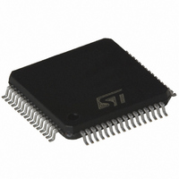
L6713A STMicroelectronics, L6713A Datasheet - Page 53

L6713A
Manufacturer Part Number
L6713A
Description
IC CTRLR 2/3PH W/DRIVERS 64-TQFP
Manufacturer
STMicroelectronics
Datasheet
1.L6713ATR.pdf
(64 pages)
Specifications of L6713A
Applications
Controller, Intel VR10, VR11, AMD CPU
Voltage - Input
12V
Number Of Outputs
3
Voltage - Output
0.3 ~ 1.6 V
Operating Temperature
0°C ~ 70°C
Mounting Type
Surface Mount
Package / Case
64-TQFP Exposed Pad, 64-eTQFP, 64-HTQFP, 64-VQFP
Output Current
2 A
Mounting Style
SMD/SMT
Maximum Operating Temperature
+ 125 C
Minimum Operating Temperature
0 C
Lead Free Status / RoHS Status
Lead free / RoHS Compliant
Available stocks
Company
Part Number
Manufacturer
Quantity
Price
L6713A
Removing the dependence from the error amplifier gain, so assuming this gain high enough,
and with further simplifications, the control loop gain results:
The system control loop gain
to minimize static error and to cross the 0dB axes with a constant -20dB/dec slope with the
desired crossover frequency ω
zero and two poles; both the poles are fixed once the output filter is designed (LC filter
resonance ω
Figure 26. Equivalent control loop block diagram (left) and bode diagram (right)
To obtain the desired shape an R
implementation. A zero at ω
integrator minimizes the static error while placing the zero ω
C resonance assures a simple -20dB/dec shape of the gain.
In fact, considering the usual value for the output filter, the LC resonance results to be at
frequency lower than the above reported zero.
Compensation network can be simply designed placing ω
over frequency ω
1/10th of the switching frequency F
Moreover, it is suggested to filter the high frequency ripple on the COMP pin adding also a
capacitor between COMP pin and FB pin (it does not change the system bandwidth:
DROOP
Z
F
(s)
G
FB
LOOP
Z
FB
(s)
VREF
LC
R
F
s ( )
C
) and the zero (ω
P
R
=
FB
T
COMP
as desired obtaining (always considering that ω
–
C
4
-- -
5
F
⋅
--------------------- -
ΔV
V
R
OSC
IN
VSEN
F
PWM
=
⋅
F
Z
---------------
=1/R
R
--------------------------------- -
R
(See Figure
F
FB
T
FB
s ( )
. Neglecting the effect of Z
ESR
d V
FBG
⋅
F
V
⋅
F
OUT
R
------------------------------------------- -
ΔV
-C
C
IN
C
SW
O
) is fixed by ESR and the Droop resistance.
P
F
F
R
OSC
+
L / N
):
O
is then introduced together with an integrator. This
=
R
series network is considered for the Z
C
DROOP
+
----------------------------------------------- -
2 π R
F
R
-------
⋅
N
26) is designed in order to obtain a high DC gain
⋅
L
5
-- - ω
4
C
=
ESR
O
⋅
⋅
-------------------- -
⋅
C
T
--------------------------------------------------------------------------------------------------------------------------------------------
s
V
R
F
O
2
OUT
⋅
1
F
⋅
------------------------------------------------------- -
N
⋅
⋅
N F
C
--- -
N
L
⋅
O
⋅
R
(
1
⋅
O
R
---- -
N
System control loop compensation
L
SW
+
DROOP
s C
+
R
⋅
s
F
F
F
[dB]
L
⋅
K
O
(s), the transfer function has one
= ω
------------------ -
N
F
⋅
dB
(
+
⋅
in correspondence with the L-
R
L
R
LC
DROOP
ESR
O
ω
+
and imposing the cross-
T
LC
C
might be not higher than
=
)
O
G
ω
LOOP
F
⋅
//R
ω
ESR
ESR
O
(s)
+
+
ESR
C
F
O
(s)
)
⋅
R
-------
N
L
Z
F
+
(s)
1
ω
53/64
T
ω


