L6713A STMicroelectronics, L6713A Datasheet - Page 37

L6713A
Manufacturer Part Number
L6713A
Description
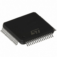
IC CTRLR 2/3PH W/DRIVERS 64-TQFP
Manufacturer
STMicroelectronics
Datasheet
1.L6713ATR.pdf
(64 pages)
Specifications of L6713A
Applications
Controller, Intel VR10, VR11, AMD CPU
Voltage - Input
12V
Number Of Outputs
3
Voltage - Output
0.3 ~ 1.6 V
Operating Temperature
0°C ~ 70°C
Mounting Type
Surface Mount
Package / Case
64-TQFP Exposed Pad, 64-eTQFP, 64-HTQFP, 64-VQFP
Output Current
2 A
Mounting Style
SMD/SMT
Maximum Operating Temperature
+ 125 C
Minimum Operating Temperature
0 C
Lead Free Status / RoHS Status
Lead free / RoHS Compliant
Available stocks
Company
Part Number
Manufacturer
Quantity
Price
L6713A
13
Load transient boost technology
Load transient boost LTB Technology™ (patent pending) is a L6713A feature to minimize
the count of output filter capacitors (MLCC and bulk capacitors) to respect the load transient
specifications.
The device turns on simultaneously all the phases as soon as a load transient is detected
and keep them on for the necessary time to supply the extra energy to the load. This time
depends on the COMP pin voltage and on a internal gain, in order to keep under control the
output voltage ring back.
Load transition is detected through LTB™ pin connecting a R
measures the derivate dV/dt of the output voltage and so it is able to turns on all the phases
immediately after a load transition detection, minimizing the delay intervention.
Modifying the R
design flexibility
where dV
Moreover, load transient boost LTB Technology™ gain can be easily modified in order to
keep under control the output voltage ring back.
Figure 12. LTB connections (left) and waveform (right)
Short LTB pin to SGND to disable the LTB Technology™: in this condition the device works
as a dual-edge asynchronous PWM controller.
LTB
OUT
is the output voltage drop due to load transition.
R
LTB
LTB
-C
LTB
C
LTB
values the dV/dt can be easily programmed, extending the system
C
To VCC_Core
LTB
=
R
LTB
----------------------------------------------------- -
2 π R
⋅
=
⋅
dV
----------------- -
50μA
LTB
1
OUT
⋅
N F
Load transient boost technologyTM
⋅
TM
SW
LTB
-C
LTB
vs. VOUT: the device
37/64


