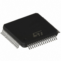
L6713A STMicroelectronics, L6713A Datasheet - Page 55

L6713A
Manufacturer Part Number
L6713A
Description
IC CTRLR 2/3PH W/DRIVERS 64-TQFP
Manufacturer
STMicroelectronics
Datasheet
1.L6713ATR.pdf
(64 pages)
Specifications of L6713A
Applications
Controller, Intel VR10, VR11, AMD CPU
Voltage - Input
12V
Number Of Outputs
3
Voltage - Output
0.3 ~ 1.6 V
Operating Temperature
0°C ~ 70°C
Mounting Type
Surface Mount
Package / Case
64-TQFP Exposed Pad, 64-eTQFP, 64-HTQFP, 64-VQFP
Output Current
2 A
Mounting Style
SMD/SMT
Maximum Operating Temperature
+ 125 C
Minimum Operating Temperature
0 C
Lead Free Status / RoHS Status
Lead free / RoHS Compliant
Available stocks
Company
Part Number
Manufacturer
Quantity
Price
L6713A
23
23.1
Tolerance band (TOB) definition
Output voltage load-line varies considering component process variation, system
temperature extremes, and age degradation limits. Moreover, individual tolerance of the
components also varies among designs: it is then possible to define a manufacturing
tolerance band (TOB
nominal load line characteristic.
TOB
current sense circuit tolerance and time constant matching error tolerance. All these
parameters can be composed thanks to the RSS analysis so that the manufacturing
variation on TOB results to be:
Output voltage ripple (V
to the manufacturing TOB in order to get the system tolerance band as follow:
All the component spreads and variations are usually considered at 3σ. Here follows an
explanation on how to calculate these parameters for a reference L6713A application.
Controller tolerance (TOB
It can be further sliced as follow:
●
●
Controller tolerance results then to be:
Manuf
Reference tolerance. L6713A is trimmed during the production stage to ensure the
output voltage to be within k
line variations. In addition, the device automatically adds a -19 mV offset (Only for Intel
mode) avoiding the use of any external component. This offset is already included
during the trimming process in order to avoid the use of any external circuit to generate
this offsets and, moreover, avoiding the introduction of any further error to be
considered in the TOB calculation.
Current reading circuit. The device reads the current flowing across the inductor DCR
by using its dedicated differential inputs. The current sourced by the VRD is then
reproduced and sourced from the DROOP pin scaled down by a proper designed gain
as follow:
This current multiplied by the R
programming the droop function according to the selected DCR/Rg gain and R
resistor. Deviations in the current sourced due to errors in the current reading, impacts
on the output voltage depending on the size of R
during the production stage in order to guarantee a maximum deviation of k
from the nominal value.
can be sliced into different three main categories: Controller tolerance, external
TOB
TOB
Manuf
Manuf
Controller
P
=V
) that defines the possible output voltage spread across the
=
PP
/2) and temperature measurement error (V
TOB
=
TOB
VID
[
2
Controller
I
(
= ± 0.5 % (± 0.6 % for AMD DAC) over temperature and
DROOP
FB
VID 19mV
=
Controller
resistor connected from FB pin vs. the load allows
TOB
–
=
+
Manuf
TOB
DCR
------------ - I
Rg
) k
⋅
+
2
CurrSense
)
⋅
VID
V
OUT
P
FB
+
]
2
V
resistor. The device is trimmed
+
Tolerance band (TOB) definition
TC
(
k
+
IDROOP
TOB
2
TCMatching
⋅
R
FB
)
TC
2
) must be added
IFB
= ± 1 μA
FB
55/64


