L6713A STMicroelectronics, L6713A Datasheet - Page 35

L6713A
Manufacturer Part Number
L6713A
Description
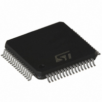
IC CTRLR 2/3PH W/DRIVERS 64-TQFP
Manufacturer
STMicroelectronics
Datasheet
1.L6713ATR.pdf
(64 pages)
Specifications of L6713A
Applications
Controller, Intel VR10, VR11, AMD CPU
Voltage - Input
12V
Number Of Outputs
3
Voltage - Output
0.3 ~ 1.6 V
Operating Temperature
0°C ~ 70°C
Mounting Type
Surface Mount
Package / Case
64-TQFP Exposed Pad, 64-eTQFP, 64-HTQFP, 64-VQFP
Output Current
2 A
Mounting Style
SMD/SMT
Maximum Operating Temperature
+ 125 C
Minimum Operating Temperature
0 C
Lead Free Status / RoHS Status
Lead free / RoHS Compliant
Available stocks
Company
Part Number
Manufacturer
Quantity
Price
L6713A
12
12.1
Voltage positioning
Output voltage positioning is performed by selecting the reference DAC and by
programming the droop function and offset to the reference
sourced from DROOP and sunk from VSEN pins cause the output voltage to vary according
to the external R
The output voltage is then driven by the following relationship:
DROOP function can be disabled as well as the OFFSET: connecting DROOP pin and FB
pin together implements the load regulation dependence while, if this effect is not desired,
by shorting DROOP pin to SGND it is possible for the device to operate as a classic voltage
mode buck converter. The DROOP pin can also be connected to SGND through a resistor
obtaining a voltage proportional to the delivered current usable for monitoring purposes.
OFFSET can be disabled by using R
Figure 11. Voltage positioning (left) and droop function (right)
Offset (Optional)
The I
offset (V
VOUT, as shown in the
already introduced during the production stage for the Intel VR10,VR11 mode.
The output voltage is then programmed as follow:
Offset resistor can be designed by considering the following relationship:
Offset automatically given by the DAC selection differs from the offset implemented through
the I
(± 0.6 % for the AMD DAC) over load and line variations.
V
GND DROP
RECOVERY
PROG
To GND_core
OFFSET
(Remote Sense)
OFFSET
OS
FBG
FBG
) for the output voltage by connecting a resistor R
current: the built-in feature is trimmed in production and assures ± 0.5 % error
current
V
V
OUT
OUT
To VCC_core
(Remote Sense)
FB
R
OFFSET
and R
=
=
V
(See Table
REF
VSEN
VSEN
V
V
REF
REF
Figure
OFFSET
I
OFFSET
–
–
R
V
DROOP
FB
(
(
R
REF
R
11; this offset has to be considered in addition to the one
FB
FB
5) sunk from the VSEN pin allows programming a positive
resistor.
+
+
=
I
DROOP
R
R
R
⎧
⎨
⎩
OFFSET
OFFSET
OFFSET
OFFSET
VID 19mV
VID
FB
–
equal to zero.
)
)
⋅
⋅
R
=
ERROR AMPLIFIER
(
F
(
I
I
DROOP
DROOP
--------------------- -
I
OFFSET
C
P
V
VR10 - VR11
AMD 6BIT
C
OS
F
COMP
)
)
+
+
(
(
R
R
OFFSET
OFFSET
(See Figure
OFFSET
V
V
V
NOM
MAX
MIN
RESPONSE WITHOUT DROOP
)
)
RESPONSE WITH DROOP
⋅
⋅
between VSEN pin and
(
(
I
I
OFFSET
OFFSET
Voltage positioning
11). The currents
ESR Drop
)
)
35/64


