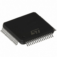
L6713A STMicroelectronics, L6713A Datasheet - Page 30

L6713A
Manufacturer Part Number
L6713A
Description
IC CTRLR 2/3PH W/DRIVERS 64-TQFP
Manufacturer
STMicroelectronics
Datasheet
1.L6713ATR.pdf
(64 pages)
Specifications of L6713A
Applications
Controller, Intel VR10, VR11, AMD CPU
Voltage - Input
12V
Number Of Outputs
3
Voltage - Output
0.3 ~ 1.6 V
Operating Temperature
0°C ~ 70°C
Mounting Type
Surface Mount
Package / Case
64-TQFP Exposed Pad, 64-eTQFP, 64-HTQFP, 64-VQFP
Output Current
2 A
Mounting Style
SMD/SMT
Maximum Operating Temperature
+ 125 C
Minimum Operating Temperature
0 C
Lead Free Status / RoHS Status
Lead free / RoHS Compliant
Available stocks
Company
Part Number
Manufacturer
Quantity
Price
Power dissipation
9
30/64
Power dissipation
L6713A embeds high current MOSFET drivers for both high side and low side MOSFETs: it
is then important to consider the power the device is going to dissipate in driving them in
order to avoid overcoming the maximum junction operative temperature. In addition, since
the device has an exposed pad to better dissipate the power, the thermal resistance
between junction and ambient consequent to the layout is also important: thermal pad
needs to be soldered to the PCB ground plane through several VIAs in order to facilitate the
heat dissipation.
Two main terms contribute in the device power dissipation: bias power and drivers' power.
The first one (P
and it is simply quantifiable as follow (assuming to supply HS and LS drivers with the same
VCC of the device):
where N is the number of phases.
Drivers' power is the power needed by the driver to continuously switch on and off the
external MOSFETs; it is a function of the switching frequency and total gate charge of the
selected MOSFETs. It can be quantified considering that the total power P
switch the MOSFETs (easy calculable) is dissipated by three main factors: external gate
resistance (when present), intrinsic MOSFET resistance and intrinsic driver resistance. This
last term is the important one to be determined to calculate the device power dissipation.
The total power dissipated to switch the MOSFETs results:
External gate resistors helps the device to dissipate the switching power since the same
power P
resulting in a general cooling of the device. When driving multiple MOSFETs in parallel, it is
suggested to use one gate resistor for each MOSFET.
SW
will be shared between the internal driver impedance and the external resistor
DC
) depends on the static consumption of the device through the supply pins
P
SW
P
=
DC
N F
=
⋅
V
SW
CC
⋅
⋅
(
(
Q
I
CC
GHS
+
⋅
N I
V
⋅
BOOT
CCDRx
+
Q
+
GLS
N I
⋅
⋅
BOOTx
V
CCDRx
)
)
SW
dissipated to
L6713A


