MCZ33927EK Freescale Semiconductor, MCZ33927EK Datasheet - Page 9
MCZ33927EK
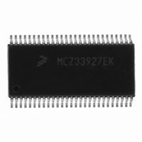
Manufacturer Part Number
MCZ33927EK
Description
IC FET PRE-DRIVER 3PH 54-SOIC
Manufacturer
Freescale Semiconductor
Specifications of MCZ33927EK
Configuration
3 Phase Bridge
Input Type
Inverting and Non-Inverting
Delay Time
265ns
Current - Peak
600mA
Number Of Configurations
1
Number Of Outputs
3
High Side Voltage - Max (bootstrap)
75V
Voltage - Supply
8 V ~ 40 V
Operating Temperature
-40°C ~ 125°C
Mounting Type
Surface Mount
Package / Case
54-SOIC (7.5mm Width) Exposed Pad, 54-eSOIC, 54-HSOIC
Lead Free Status / RoHS Status
Lead free / RoHS Compliant
Available stocks
Company
Part Number
Manufacturer
Quantity
Price


Table 3. Static Electrical Characteristics (continued)
values noted reflect the approximate parameter means at T
Analog Integrated Circuit Device Data
Freescale Semiconductor
CHARGE PUMP
GATE DRIVE
Notes
Charge Pump
Charge Pump Output Voltage
High-Side Driver On-Resistance (Sourcing)
High-Side Driver On-Resistance (Sinking)
High-Side Current Injection Allowed Without Malfunction
Low-Side Driver On-Resistance (Sourcing)
Low-Side Driver On-Resistance (Sinking)
Low-Side Current Injection Allowed Without Malfunction
Gate Source Voltage, V
High-Side Gate Drive Output Leakage Current, Per Output
13.
14.
15.
16.
17.
18.
Characteristics noted under conditions 8.0V ≤ V
High-Side Switch On-Resistance
Low-Side Switch On-Resistance
Regulation Threshold Difference
I
I
V
V
V
V
V
V
High-Side, I
Low-Side, I
OUT
OUT
PWR
PWR
PWR
PWR
PWR
PWR
When VLS is this amount below the normal VLS linear regulation threshold, the pump is enabled.
With recommended external components (1.0µF, MUR 120 diode). The Charge Pump is designed to supply the gate currents of a
system with 100A FETs in a 12V application.
This parameter is a design characteristic, not production tested.
Current injection only occurs during output switch transitions. The IC is immune to specified injected currents for a duration of
approximately 1 µs after an output switch transition. 1 µs is sufficient for all intended applications of this IC.
If a slightly higher gate voltage is required, larger bootstrap capacitors are required. At high duty cycles, the bootstrap voltage may not
recover completely, leading to a higher output on-resistance. This effect can be minimized by using low ESR capacitors for the bootstrap
and the VLS capacitors.
A small internal charge pump will supply up to 30 µA nominal to compensate for leakage on the high-side FET gate output and maintain
voltages after bootstrap events. It is not intended for external components to be connected to the High-Side FET gate, but small amounts
of additional leakage can be accommodated.
= 40mA, 6.0V < V
= 40mA, V
= V
= V
= V
= V
= V
= V
BAT
BAT
BAT
BAT
BAT
BAT
GATE
GATE
= 16V,
= 16V,
= 16V
= 16V,
= 16V,
= 16 V
BAT
= 0
= 0
> = 8.0V
PWR
(17)
-40°C ≤ T
25°C < T
-40°C ≤ T
25°C < T
BAT
Characteristic
= V
(14)
< 8.0V
BAT
,
(15)
A
A
A
A
(13)(15)
= 40V
≤ 125°C
≤ 125°C
≤ 25°C
≤ 25°C
PWR
(15)
(15)
(18)
,
,
(16)
= V
(16)
BAT
A
= 25°C under nominal conditions unless otherwise noted.
≤ 40V, -40°C ≤ T
R
R
R
R
DS(on)_H_SINK
DS(on)_H_SRC
DS(on)_L_SINK
R
DS(on)_L_SRC
R
I
Symbol
V
DS(on)_HS
HS_LEAK
DS(on)_LS
I
I
V
V
HS_INJ
LS_INJ
THREG
V
GS_H
GS_L
CP
A
≤ 125°C, unless otherwise noted. Typical
Min
250
8.5
12
13
13
–
–
–
–
–
–
–
–
–
–
–
STATIC ELECTRICAL CHARACTERISTICS
ELECTRICAL CHARACTERISTICS
14.8
15.4
Typ
500
6.0
5.0
9.5
–
–
–
–
–
–
–
–
–
–
Max
16.5
900
9.4
6.0
8.5
3.0
0.5
6.0
8.5
3.0
0.5
10
17
18
–
–
Unit
mV
µA
Ω
Ω
Ω
Ω
Ω
Ω
V
A
Α
V
33927
9
Related parts for MCZ33927EK
Image
Part Number
Description
Manufacturer
Datasheet
Request
R

Part Number:
Description:
Manufacturer:
Freescale Semiconductor, Inc
Datasheet:
Part Number:
Description:
Manufacturer:
Freescale Semiconductor, Inc
Datasheet:
Part Number:
Description:
Manufacturer:
Freescale Semiconductor, Inc
Datasheet:
Part Number:
Description:
Manufacturer:
Freescale Semiconductor, Inc
Datasheet:
Part Number:
Description:
Manufacturer:
Freescale Semiconductor, Inc
Datasheet:
Part Number:
Description:
Manufacturer:
Freescale Semiconductor, Inc
Datasheet:
Part Number:
Description:
Manufacturer:
Freescale Semiconductor, Inc
Datasheet:
Part Number:
Description:
Manufacturer:
Freescale Semiconductor, Inc
Datasheet:
Part Number:
Description:
Manufacturer:
Freescale Semiconductor, Inc
Datasheet:
Part Number:
Description:
Manufacturer:
Freescale Semiconductor, Inc
Datasheet:
Part Number:
Description:
Manufacturer:
Freescale Semiconductor, Inc
Datasheet:
Part Number:
Description:
Manufacturer:
Freescale Semiconductor, Inc
Datasheet:
Part Number:
Description:
Manufacturer:
Freescale Semiconductor, Inc
Datasheet:
Part Number:
Description:
Manufacturer:
Freescale Semiconductor, Inc
Datasheet:
Part Number:
Description:
Manufacturer:
Freescale Semiconductor, Inc
Datasheet: