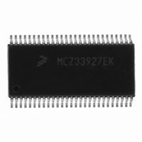
MCZ33927EK Freescale Semiconductor, MCZ33927EK Datasheet - Page 28

MCZ33927EK
Manufacturer Part Number
MCZ33927EK
Description
IC FET PRE-DRIVER 3PH 54-SOIC
Manufacturer
Freescale Semiconductor
Specifications of MCZ33927EK
Configuration
3 Phase Bridge
Input Type
Inverting and Non-Inverting
Delay Time
265ns
Current - Peak
600mA
Number Of Configurations
1
Number Of Outputs
3
High Side Voltage - Max (bootstrap)
75V
Voltage - Supply
8 V ~ 40 V
Operating Temperature
-40°C ~ 125°C
Mounting Type
Surface Mount
Package / Case
54-SOIC (7.5mm Width) Exposed Pad, 54-eSOIC, 54-HSOIC
Lead Free Status / RoHS Status
Lead free / RoHS Compliant
Available stocks
Company
Part Number
Manufacturer
Quantity
Price
RESET AND ENABLE
in
EN2), which together with the status of the VDD and VLS,
control the behavior of the IC.
following three modes:
The current consumption of the IC is at minimum.
Table 6. Functional Ratings
28
Table 5. Functions of RST, EN1 and EN2 Pins
33927
FUNCTIONAL DEVICE OPERATION
OPERATIONAL MODES
Notes
Default State of input pin Px_LS, EN1, EN2, RST, SI, SCLK, if left open
(Driver output is switched off, high impedance mode)
Default State of input pin Px_HS, CS if left open
(Driver output is switched off, high impedance mode)
0
1
1
49.
RST
Table
The 33927 has three power modes of operation described
The operating status of the IC can be described by the
Sleep Mode - When RST is low, the IC is in Sleep Mode.
• After entry to Enable Mode, the IC requires a pulse on
(
T
J
Px_LS in order to charge the bootstrap capacitor before
allowing the Px_HS to turn on. This pulse should be
about 50 µs to guarantee the bootstrap capacitor is
charged, but the IC does not enforce this condition. If
=-40°C to 150°C and supply voltage range V
To assure a defined status for all inputs, these pins are internally biased by pull-up/down current sources.
5. There are three global control inputs (RST, EN1,
EN1, EN2
0x
x0
11
xx
Sleep Mode - in this mode (low quiescent current) the driver output stage is switched-off with a weak pull-down. All error
and SPI registers are cleared. The internal 5.0V regulator is turned off and VDD is pulled low. Logic outputs are clamped
to GND.
Standby Mode - IC fully biased up and all functions are operating, the output drivers actively turn off all of the external
FETs. The SPI port is functional. Logic level outputs are driven with low impedance. V
regulators are all operating. The IC is ready to move to Enable Mode.
Enable Mode - (normal operation). Drivers are enabled; output stages follow the input command. After Enable, outputs
require a pulse on Px_LS before corresponding HS outputs will turn on in order to recharge bootstrap capacitor. All error
pin and register bits are active if detected.
FUNCTIONAL DEVICE OPERATION
(49)
BAT
Characteristic
= V
OPERATIONAL MODES
PWR
Mode of Operation (Driver Condition)
= 5.0V to 45V, C = 0.47µF)
(49)
• Standby Mode - The RST input is high while one of the
• Enable Mode - In order to enter the Enable Mode
Enable inputs is low. The IC is fully biased up and
operating, all the external FETs are actively turned off
by both high-side and low-side gate drives. The IC is
ready to enter the Enable Mode.
(normal mode of operation), and to operate the outputs,
the RST input must be high, and both Enable inputs
EN1 and EN2 must also be high.
there is an alternate means of pre-charging the
bootstrap capacitor, i.e. an external resistor from
Px_HS_S to GND, then a very brief pulse of 1.0 µs is
sufficient to reset the logic.
Analog Integrated Circuit Device Data
DD
, Charge Pump and V
Freescale Semiconductor
High (>2.0V)
Low (<1.0V)
Value
LS


