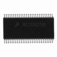
MCZ33927EK Freescale Semiconductor, MCZ33927EK Datasheet - Page 21

MCZ33927EK
Manufacturer Part Number
MCZ33927EK
Description
IC FET PRE-DRIVER 3PH 54-SOIC
Manufacturer
Freescale Semiconductor
Specifications of MCZ33927EK
Configuration
3 Phase Bridge
Input Type
Inverting and Non-Inverting
Delay Time
265ns
Current - Peak
600mA
Number Of Configurations
1
Number Of Outputs
3
High Side Voltage - Max (bootstrap)
75V
Voltage - Supply
8 V ~ 40 V
Operating Temperature
-40°C ~ 125°C
Mounting Type
Surface Mount
Package / Case
54-SOIC (7.5mm Width) Exposed Pad, 54-eSOIC, 54-HSOIC
Lead Free Status / RoHS Status
Lead free / RoHS Compliant
Available stocks
Company
Part Number
Manufacturer
Quantity
Price
reference for the SPI port. A 0.47µF (min) decoupling
capacitor must be connected to this pin.
supply only a small (1mA) external load current.
the voltage rises above the threshold, the internal logic will be
reset; driver outputs will be tri-stated and SPI communication
disabled.
signal low. The VDD regulator is powered from the VPWR
pin.
PHASE B HIGH-SIDE CONTROL INPUT (PB_HS)
driver for Phase B. The signal is active low, and is pulled up
by an internal current source.
PHASE B LOW-SIDE INPUT (PB_LS)
driver for Phase B. The signal is active high, and is pulled
down by an internal current sink.
INTERRUPT (INT)
is detected, this pin will pull high until it is cleared by
executing the Clear Interrupt command via the SPI port. The
faults capable of causing an interrupt can be masked via the
MASK0 and MASK1 SPI registers to customize the
response.
CHIP SELECT (CS)
and enables the SPI port. This signal is active low, and is
pulled up by an internal current source.
SERIAL IN (SI)
Clocked on the falling edge of SCLK, it is the most significant
bit (MSB) first. This pin is pulled down by an internal current
sink.
SERIAL CLOCK (SCLK)
SCLK typically runs at 3 MHz (up to 5 MHz) and is pulled
down by an internal current sink.
SERIAL OUT (SO)
stated until CS is low. New data appears on rising edges of
SCLK in preparation for latching by the falling edge of SCLK
on the master.
Analog Integrated Circuit Device Data
Freescale Semiconductor
This regulator is intended for internal IC use and can
A power-on-reset (POR) circuit monitors this pin and until
The VDD regulator can be disabled by asserting the RST
This pin is the input logic signal, enabling the High-Side
This pin is the input logic signal, enabling the Low-Side
The Interrupt pin is a totem pole logic output. When a fault
Chip select is a logic input that frames the SPI commands
The Serial In pin is used to input data to the SPI port.
This logic input is the clock is used for the SPI port. The
Output data for the SPI port streams from this pin. It is tri-
PHASE C LOW-SIDE INPUT (PC_LS)
C. This pin is an active high, and is pulled down by an internal
current sink.
PHASE C HIGH-SIDE INPUT (PC_HS)
C. This signal is active low, and is pulled up by an internal
current source.
AMPLIFIER OUTPUT (AMP_OUT)
also the sense input to the overcurrent comparator.
AMPLIFIER INVERTING INPUT (AMP_N)
AMPLIFIER NON-INVERTING INPUT (AMP_P)
OVERCURRENT COMPARATOR OUTPUT
(OC_OUT)
level output. A logic high indicates an overcurrent condition.
OVERCURRENT COMPARATOR THRESHOLD
(OC_TH)
comparator.
VOLTAGE SOURCE SUPPLY (VSS)
power supplies.
GROUND (GND0,GND1)
resistor. They provide device substrate connections and also
the primary return path for ESD protection.
VLS REGULATOR CAPACITOR (VLS_CAP)
impedance for switching currents on the gate drive. A low
ESR decoupling capacitor, capable of sourcing the pulsed
drive currents must be connected between this pin and VSS.
placed on the opposite end of the IC to minimize the source
impedance to the gate drive circuits.
PHASE C GROUND (PGNDC)
gate currents from the low side FET. Best performance is
normally realized by connecting this node directly to the
source of the low side FET for phase C.
This input logic pin enables the Low-Side Driver for Phase
This input logic pin enables the High-Side Driver for Phase
This pin is the output for the current sensing amplifier. It is
The inverting input to the current sensing amplifier.
The non-inverting input to the current sensing amplifier.
The overcurrent comparator output is a totem pole logic
This input sets the threshold level of the overcurrent
VSS is the ground reference for the logic interface and
These two pins are connected internally to VSS by a 1.0 Ω
This connection is for a capacitor which will provide a low
This is the same DC node as VLS, but it is physically
The phase C power ground is the pin used to return the
FUNCTIONAL DESCRIPTIONS
INTRODUCTION
33927
21


