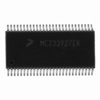
MCZ33927EK Freescale Semiconductor, MCZ33927EK Datasheet - Page 10

MCZ33927EK
Manufacturer Part Number
MCZ33927EK
Description
IC FET PRE-DRIVER 3PH 54-SOIC
Manufacturer
Freescale Semiconductor
Specifications of MCZ33927EK
Configuration
3 Phase Bridge
Input Type
Inverting and Non-Inverting
Delay Time
265ns
Current - Peak
600mA
Number Of Configurations
1
Number Of Outputs
3
High Side Voltage - Max (bootstrap)
75V
Voltage - Supply
8 V ~ 40 V
Operating Temperature
-40°C ~ 125°C
Mounting Type
Surface Mount
Package / Case
54-SOIC (7.5mm Width) Exposed Pad, 54-eSOIC, 54-HSOIC
Lead Free Status / RoHS Status
Lead free / RoHS Compliant
Available stocks
Company
Part Number
Manufacturer
Quantity
Price
Table 3. Static Electrical Characteristics (continued)
values noted reflect the approximate parameter means at T
10
33927
ELECTRICAL CHARACTERISTICS
STATIC ELECTRICAL CHARACTERISTICS
OVERCURRENT COMPARATOR
HOLD OFF CIRCUIT
PHASE COMPARATOR
DESATURATION DETECTOR
CURRENT SENSE AMPLIFIER
Notes
Common Mode Input Range
Input Offset Voltage
Overcurrent Comparator Threshold Hysteresis
Output Voltage
V
Hold Off Current (At Each GATE Pin)
High-Level Input Voltage Threshold
Low-Level Input Voltage Threshold
High-Level Output Voltage at I
Low-Level Output Voltage at I
High-Side Source Input Resistance
Desaturation Detector Threshold
Recommended External Series Resistor (See
Recommended External Feedback Resistor (See
Maximum Input Differential Voltage (See
Input Common Mode Range
Input Offset Voltage
Input Offset Voltage Drift
Input Bias Current
19.
20.
21.
22.
23.
Characteristics noted under conditions 8.0V ≤ V
DD
High-Level at I
Low-Level at I
RST pin High
3.0V < V
Limited by the Output Voltage Dynamic Range
V
R
V
ID
CM
Threshold (V
S
This parameter is a design characteristic, not production tested.
The hold off circuit is designed to operate over the full operating range of V
production test.
Desaturation is measured as the voltage drop below V
high-side FET. See
As long as one input is within V
a phase inversion on the output.
Input resistance is impedance from high-side source and is referenced to ground. Approximate tolerance is ±20%.
= 1kΩ, V
= V
= 2.0V
AMP_P
BAT
CM
< 40V
OL
- V
OH
DD
= 0.0V
= 500µA
AMP_N
= -500µA
Falling)
(20)
(19)
Figure
Characteristic
(19),
OL
OH
(22)
(21)
= 500µA
5.
= -500µA
(19),
CM
(23)
the output is guaranteed to have the correct phase. Exceeding the common mode rails will not cause
Figure
Figure
(19)
9)
Figure
9)
PWR
9)
= V
BAT
BAT
, thus the threshold is compared to the drain-source voltage of the external
A
= 25°C under nominal conditions unless otherwise noted.
≤ 40V, -40°C ≤ T
V
V
δV
Symbol
V
V
OC_HYST
V
V
I
DES_TH
OS_OC
V
V
DD_TH
HOLD
V
V
V
V
R
V
IH_TH
IL_TH
R
V
OS
R
CΜ
I
CM
OH
OH
OS
OL
OL
FB
b
IN
ID
S
BAT
/δT
. The specification indicates the conditions used in
A
≤ 125°C, unless otherwise noted. Typical
0.85 V
0.85 V
0.5 V
0.3 V
-800
-200
Min
2.0
-50
1.5
1.2
5.0
-15
50
10
–
–
–
–
0
–
BAT
BAT
DD
DD
Analog Integrated Circuit Device Data
Typ
-10
1.4
1.0
50
–
–
–
–
–
–
–
–
–
–
–
–
–
–
–
Freescale Semiconductor
0.65 V
0.45 V
V
DD
+800
+200
Max
V
V
300
300
+15
0.5
4.0
0.5
1.6
3.0
50
15
DD
DD
–
–
–
-0.02
BAT
BAT
µV/°C
Unit
mV
mV
mV
mV
µA
kΩ
kΩ
kΩ
nA
V
V
V
V
V
V
V
V
V


