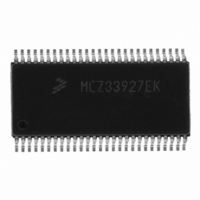
MCZ33927EK Freescale Semiconductor, MCZ33927EK Datasheet - Page 27

MCZ33927EK
Manufacturer Part Number
MCZ33927EK
Description
IC FET PRE-DRIVER 3PH 54-SOIC
Manufacturer
Freescale Semiconductor
Specifications of MCZ33927EK
Configuration
3 Phase Bridge
Input Type
Inverting and Non-Inverting
Delay Time
265ns
Current - Peak
600mA
Number Of Configurations
1
Number Of Outputs
3
High Side Voltage - Max (bootstrap)
75V
Voltage - Supply
8 V ~ 40 V
Operating Temperature
-40°C ~ 125°C
Mounting Type
Surface Mount
Package / Case
54-SOIC (7.5mm Width) Exposed Pad, 54-eSOIC, 54-HSOIC
Lead Free Status / RoHS Status
Lead free / RoHS Compliant
Available stocks
Company
Part Number
Manufacturer
Quantity
Price
Phase Comparator
error is generated if the output signal (at Px_HS_S) does not
properly reflect the drive conditions.
Phase Comparator compares the voltage at the Px_HS_S
node with a reference of one half the voltage at the VBAT pin.
A high side phase error (which will also trigger the
Desaturation Detector) occurs when the high side FET is
commanded on, and Px_HS_S is still low at the end of the
deadtime and blanking time duration. Similarly, a LS phase
error occurs when the low side FET is commanded on, and
the Px_HS_S is still high at the end of the deadtime and
blanking time duration.
Analog Integrated Circuit Device Data
Freescale Semiconductor
Faults could also be detected as Phase Errors . A phase
A phase error is detected by a Phase Comparator. The
Figure 14. Short to Battery Detection
each phase. Each phase error is the OR of the high side and
low side phase errors. This flag can generate an interrupt if
the appropriate mask bit is set. The INT will be held in the
High state until the fault is removed, and the appropriate bit
in the Status Register 0 is cleared by the CLINT1 command.
This fault reporting mechanism is described in detail in the
Logic Commands and Registers
HOLD OFF CIRCUIT
absence of V
small current source, generated from VBAT, typically 100 µA,
is mirrored and pulls all the output gate drive pins low when
V
is lower than the VLS_Disable threshold.
CHARGE PUMP
elements required to implement a charge pump when
combined with external capacitors and diodes for enhanced
low voltage operation.
using the charge pump (see
for VLS includes the charge pump and a linear regulator. The
regulation set point for the linear regulator is nominally at
15.34V. As long as VLS output voltage (VLS
than the VLS analog regulator threshold (VLS
V
until VLS
with this cycle even when there is overlap in the thresholds
due to the design of the regulator system.
dependent on the pump capacitor value and quality, the
pump frequency (nominally 130kHz) and the Rdson of the
pump FETs. The effective charge voltage for the pump
capacitor would be V
transfer would then be C
Multiplying by the switch frequency gives the theoretical
current the pump can transfer: F
2*V
charge pump (Trickle Charge Pump - see
used to maintain the high-side drivers’ gate V
percent duty cycle modes.
DD
THREG
The Phase Error Flag is the triple OR of phase errors from
The IC guarantees the output FETs are turned off in the
The Charge Pump circuit provides the basic switching
When the 33927 is connected per the typical application
If VLS
V
The maximum current the charge pump can supply is
NOTE: There is also another smaller, fully integrated
DIODE
HYST
is less than about 3.0V,
, the charge pump is not active.
OUT
OUT
).
is approximately 200mV. VLS
< VLS
DD
> VLS
FUNCTIONAL INTERNAL BLOCK DESCRIPTION
or V
ATH
ATH
PWR
BAT
– V
– V
PUMP
– 2*V
by means of the Hold off circuit. A
THREG
THREG
RST
Figure
* (V
DIODE
PUMP
is active (low), or when VLS
section.
the charge pump turns ON
+ V
BAT
17), the regulation path
. The total charge
HYST
* C
– 2*V
ATH
PUMP
Figure
will not interfere
DIODE
INTRODUCTION
OUT
GS
ATH
* (V
) is greater
2), which is
in 100
) minus
).
BAT
–
33927
27


