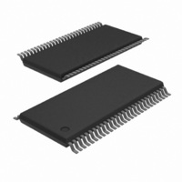
PCF8576DT/2,118 NXP Semiconductors, PCF8576DT/2,118 Datasheet - Page 43

PCF8576DT/2,118
Manufacturer Part Number
PCF8576DT/2,118
Description
IC LCD DRIVER 40/160SEG 56TSSOP
Manufacturer
NXP Semiconductors
Datasheet
1.PCF8576DT2118.pdf
(50 pages)
Specifications of PCF8576DT/2,118
Package / Case
56-TSSOP
Display Type
LCD
Configuration
40 Segment
Interface
I²C
Current - Supply
24µA
Voltage - Supply
1.8 V ~ 5.5 V
Operating Temperature
-40°C ~ 85°C
Mounting Type
Surface Mount
Number Of Digits
20
Number Of Segments
160
Maximum Clock Frequency
400 KHz
Operating Supply Voltage
1.8 V to 5.5 V
Maximum Power Dissipation
400 mW
Maximum Operating Temperature
+ 85 C
Maximum Supply Current
50 mA
Minimum Operating Temperature
- 40 C
Lead Free Status / RoHS Status
Lead free / RoHS Compliant
For Use With
568-4703 - DEMO BOARD LCD GRAPHIC DRIVER
Digits Or Characters
-
Lead Free Status / Rohs Status
Lead free / RoHS Compliant
Other names
568-3558-2
935276166118
PCF8576DT/2-T
935276166118
PCF8576DT/2-T
NXP Semiconductors
PCF8576D
Product data sheet
18.3 Wave soldering
18.4 Reflow soldering
Not all SMDs can be wave soldered. Packages with solder balls, and some leadless
packages which have solder lands underneath the body, cannot be wave soldered. Also,
leaded SMDs with leads having a pitch smaller than ~0.6 mm cannot be wave soldered,
due to an increased probability of bridging.
The reflow soldering process involves applying solder paste to a board, followed by
component placement and exposure to a temperature profile. Leaded packages,
packages with solder balls, and leadless packages are all reflow solderable.
Key characteristics in both wave and reflow soldering are:
Key characteristics in wave soldering are:
Key characteristics in reflow soldering are:
•
•
•
•
•
•
•
•
•
•
•
•
•
Through-hole components
Leaded or leadless SMDs, which are glued to the surface of the printed circuit board
Board specifications, including the board finish, solder masks and vias
Package footprints, including solder thieves and orientation
The moisture sensitivity level of the packages
Package placement
Inspection and repair
Lead-free soldering versus SnPb soldering
Process issues, such as application of adhesive and flux, clinching of leads, board
transport, the solder wave parameters, and the time during which components are
exposed to the wave
Solder bath specifications, including temperature and impurities
Lead-free versus SnPb soldering; note that a lead-free reflow process usually leads to
higher minimum peak temperatures (see
reducing the process window
Solder paste printing issues including smearing, release, and adjusting the process
window for a mix of large and small components on one board
Reflow temperature profile; this profile includes preheat, reflow (in which the board is
heated to the peak temperature) and cooling down. It is imperative that the peak
temperature is high enough for the solder to make reliable solder joints (a solder paste
characteristic). In addition, the peak temperature must be low enough that the
packages and/or boards are not damaged. The peak temperature of the package
depends on package thickness and volume and is classified in accordance with
Table 25
and
All information provided in this document is subject to legal disclaimers.
26
Rev. 10 — 14 February 2011
Universal LCD driver for low multiplex rates
Figure
30) than a SnPb process, thus
PCF8576D
© NXP B.V. 2011. All rights reserved.
43 of 50


