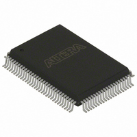
EPC4QC100N Altera, EPC4QC100N Datasheet - Page 27

EPC4QC100N
Manufacturer Part Number
EPC4QC100N
Description
IC CONFIG DEVICE 4MBIT 100-PQFP
Manufacturer
Altera
Series
EPCr
Specifications of EPC4QC100N
Programmable Type
In System Programmable
Memory Size
4Mb
Voltage - Supply
3 V ~ 3.6 V
Operating Temperature
0°C ~ 70°C
Package / Case
100-MQFP, 100-PQFP
Memory Type
Flash
Clock Frequency
66.7MHz
Supply Voltage Range
3V To 3.6V
Memory Case Style
QFP
No. Of Pins
100
Operating Temperature Range
0°C To +70°C
Access Time
90ns
Rohs Compliant
Yes
Lead Free Status / RoHS Status
Lead free / RoHS Compliant
Other names
544-1378
EPC4QC100N
EPC4QC100N
Available stocks
Company
Part Number
Manufacturer
Quantity
Price
Company:
Part Number:
EPC4QC100N
Manufacturer:
ALTERA
Quantity:
25
Company:
Part Number:
EPC4QC100N
Manufacturer:
Altera
Quantity:
135
Company:
Part Number:
EPC4QC100N
Manufacturer:
ALTERA32EOL
Quantity:
135
Chapter 1: Enhanced Configuration Devices (EPC4, EPC8, and EPC16) Data Sheet
Programming and Configuration File Support
Table 1–11. Enhanced Configuration Device JTAG Instructions
June 2011 Altera Corporation
SAMPLE/
PRELOAD
EXTEST
BYPASS
IDCODE
USERCODE
INIT_CONF
PENDCFG
Note to
(1) Enhanced configuration device instruction register length is 10 and boundary scan length is 174.
JTAG Instruction
Table
1–11:
f
00 0101 0101
00 0000 0000
11 1111 1111
00 0101 1001
00 0111 1001
00 0110 0001
00 0110 0101
The ISP circuitry in the enhanced configuration device is compliant with the IEEE Std.
1532 specification. The IEEE Std. 1532 is a standard that allows concurrent ISP
between devices from multiple vendors.
For more information about the enhanced configuration device JTAG support, refer to
the BSDL files provided at the Altera website.
Enhanced configuration devices can also be programmed by third-party flash
programmers or on-board processors using the external flash interface. Programming
files (.pof) can be converted to an Intel HEX format file (.hexout) using the Quartus II
Convert Programming Files utility, for use with the programmers or processors.
OPCODE
Allows a snapshot of the state of the enhanced configuration device pins to be
captured and examined during normal device operation and permits an initial
data pattern output at the device pins.
Allows the external circuitry and board-level interconnections to be tested by
forcing a test pattern at the output pins and capturing results at the input pins.
Places the 1-bit bypass register between the TDI and the TDO pins, which allow
the BST data to pass synchronously through a selected device to adjacent
devices during normal device operation.
Selects the device IDCODE register and places it between TDI and TDO, allowing
the device IDCODE to be serially shifted out to TDO. The device IDCODE for all
enhanced configuration devices is the same and shown below:
0100A0DDh
Selects the USERCODE register and places it between TDI and TDO, allowing the
USERCODE to be serially shifted out the TDO. The 32-bit USERCODE is a
programmable user-defined pattern.
This function initiates the FPGA re-configuration process by pulsing the
nINIT_CONF pin low, which is connected to the FPGA nCONFIG pin. After this
instruction is updated, the nINIT_CONF pin is pulsed low when the JTAG state
machine enters Run-Test/Idle state. The nINIT_CONF pin is then released
and nCONFIG is pulled high by the resistor after the JTAG state machine goes out
of Run-Test/Idle state. The FPGA configuration starts after nCONFIG goes
high. As a result, the FPGA is configured with the new configuration data stored
in flash via ISP. This function can be added to your programming file (
.jbc) in the Quartus II software by enabling the Initiate configuration after
programming option in the Programmer options window (Options menu).
This optional function can be used to hold the nINIT_CONF pin low during JTAG-
based ISP of the enhanced configuration device. This feature is useful when the
external flash interface is controlled by an external FPGA/processor. This function
prevents contention on the flash pins when both the controller and external
device try to access the flash simultaneously. Before the enhanced configuration
device’s controller can access the flash memory, the external FPGA/processor
needs to tri-state its interface to flash.This can be ensured by resetting the FPGA
using the nINIT_CONF, which drives the nCONFIG pin and keeps the external
FPGA/processor in the “reset” state. The nINIT_CONF pin is released when the
initiate configuration (INIT_CONF) JTAG instruction is issued.
(Note 1)
Description
Volume 2: Configuration Handbook
.pof , .jam,
1–27


