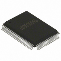
EPC4QC100N Altera, EPC4QC100N Datasheet - Page 23

EPC4QC100N
Manufacturer Part Number
EPC4QC100N
Description
IC CONFIG DEVICE 4MBIT 100-PQFP
Manufacturer
Altera
Series
EPCr
Specifications of EPC4QC100N
Programmable Type
In System Programmable
Memory Size
4Mb
Voltage - Supply
3 V ~ 3.6 V
Operating Temperature
0°C ~ 70°C
Package / Case
100-MQFP, 100-PQFP
Memory Type
Flash
Clock Frequency
66.7MHz
Supply Voltage Range
3V To 3.6V
Memory Case Style
QFP
No. Of Pins
100
Operating Temperature Range
0°C To +70°C
Access Time
90ns
Rohs Compliant
Yes
Lead Free Status / RoHS Status
Lead free / RoHS Compliant
Other names
544-1378
EPC4QC100N
EPC4QC100N
Available stocks
Company
Part Number
Manufacturer
Quantity
Price
Company:
Part Number:
EPC4QC100N
Manufacturer:
ALTERA
Quantity:
25
Company:
Part Number:
EPC4QC100N
Manufacturer:
Altera
Quantity:
135
Company:
Part Number:
EPC4QC100N
Manufacturer:
ALTERA32EOL
Quantity:
135
Chapter 1: Enhanced Configuration Devices (EPC4, EPC8, and EPC16) Data Sheet
Pin Description
Table 1–9. External Flash Interface Pins (Part 1 of 2)
June 2011 Altera Corporation
A[20..0]
DQ[15..0]
CE#
RP#
OE#
WE#
Pin Name
(1)
(1)
Bidirectional
Pin Type
Input
Input
Input
Input
Input
These pins are the address input to the flash memory for read and write
operations. The addresses are internally latched during a write cycle.
When the external flash interface is not used, leave these pins floating (with a few
exceptions (1)). These flash address, data, and control pins are internally
connected to the configuration controller.
In the 100-pin PQFP package, four address pins (A0, A1, A15, A16) are not
internally connected to the controller. These loop-back connections must be made
on the board between the C-A[] and F-A[] pins even when not using the external
flash interface. All other address pins are connected internal to the package.
All address pins are connected internally in the 88-pin UFBGA package.
Pin A20 in EPC16 devices, pins A20 and A19 in EPC8 devices, and pins A20, A19,
and A18 in EPC4 devices are no-connects. These pins should be left floating on
the board.
This is the flash data bus interface between the flash memory and the controller.
The controller or an external source drives DQ[15..0] during the flash command
and the data write bus cycles. During the data read cycle, the flash memory drives
the DQ[15..0] to the controller or external device.
Leave these pins floating on the board when the external flash interface is not
used.
Active low flash input pin that activates the flash memory when asserted. When it
is high, it deselects the device and reduces power consumption to standby levels.
This flash input pin is internally connected to the controller.
Leave this pin floating on the board when the external flash interface is not used.
Active low flash input pin that resets the flash when asserted. When high, it
enables normal operation. When low, it inhibits write operation to the flash
memory, which provides data protection during power transitions.
This flash input is not internally connected to the controller. Hence, an external
loop-back connection between C-RP# and F-RP# must be made on the board
even when you are not using the external flash interface.
When using the external flash interface, connect the external device to the RP# pin
with the loop back. Always tri-state RP# when the flash is not in use.
Active-low flash-control input that is asserted by the controller or external device
during flash read cycles. When asserted, it enables the drivers of the flash output
pins.
Leave this pin floating on the board when the external flash interface is not used.
Active-low flash-write strobe asserted by the controller or external device during
flash write cycles. When asserted, it controls writes to the flash memory. In the
flash memory, addresses and data are latched on the rising edge of the WE# pulse.
This flash input is not internally connected to the controller. Hence, an external
loop-back connection between C-WE# and F-WE# must be made on the board
even when you are not using the external flash interface.
When using the external flash interface, connect the external device to the WE# pin
with the loop back.
Description
Volume 2: Configuration Handbook
1–23


