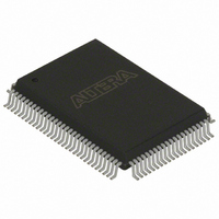
EPC4QC100N Altera, EPC4QC100N Datasheet - Page 22

EPC4QC100N
Manufacturer Part Number
EPC4QC100N
Description
IC CONFIG DEVICE 4MBIT 100-PQFP
Manufacturer
Altera
Series
EPCr
Specifications of EPC4QC100N
Programmable Type
In System Programmable
Memory Size
4Mb
Voltage - Supply
3 V ~ 3.6 V
Operating Temperature
0°C ~ 70°C
Package / Case
100-MQFP, 100-PQFP
Memory Type
Flash
Clock Frequency
66.7MHz
Supply Voltage Range
3V To 3.6V
Memory Case Style
QFP
No. Of Pins
100
Operating Temperature Range
0°C To +70°C
Access Time
90ns
Rohs Compliant
Yes
Lead Free Status / RoHS Status
Lead free / RoHS Compliant
Other names
544-1378
EPC4QC100N
EPC4QC100N
Available stocks
Company
Part Number
Manufacturer
Quantity
Price
Company:
Part Number:
EPC4QC100N
Manufacturer:
ALTERA
Quantity:
25
Company:
Part Number:
EPC4QC100N
Manufacturer:
Altera
Quantity:
135
Company:
Part Number:
EPC4QC100N
Manufacturer:
ALTERA32EOL
Quantity:
135
1–22
Pin Description
Table 1–8. Configuration Interface Pins
Volume 2: Configuration Handbook
DATA[7..0]
DCLK
nCS
nINIT_CONF
OE
Pin Name
Output
Output
Input
Open-Drain Output
Open-Drain
Bidirectional
Table 1–8
tables include configuration interface pins, external flash interface pins, JTAG
interface pins, and other pins.
Pin Type
through
Configuration data output bus. DATA changes on each falling edge of DCLK. DATA
is latched into the FPGA on the rising edge of DCLK.
The DCLK output pin from the enhanced configuration device serves as the FPGA
configuration clock. DATA is latched by the FPGA on the rising edge of DCLK.
The nCS pin is an input to the enhanced configuration device and is connected to
the FPGA’s CONF_DONE signal for error detection after all configuration data is
transmitted to the FPGA. The FPGA will always drive nCS and OE low when
nCONFIG is asserted. This pin contains a programmable internal weak pull-up
resistor of 6K that can be disabled/enabled in the Quartus II software through
the Disable nCS and OE pull-ups on configuration device option.
The nINIT_CONF pin can be connected to the nCONFIG pin on the FPGA to
initiate configuration from the enhanced configuration device via a private JTAG
instruction. This pin contains an internal weak pull-up resistor of 6K that is
always active. The INIT_CONF pin does not need to be connected if its
functionality is not used. If n
V
This pin is driven low when POR is not complete. A user-selectable 2-ms or
100-ms counter holds off the release of OE during initial power up to permit
voltage levels to stabilize. POR time can be extended by externally holding OE low.
OE is connected to the FPGA nSTATUS signal. After the enhanced configuration
device controller releases OE, it waits for the nSTATUS-OE line to go high before
starting the FPGA configuration process. This pin contains a programmable
internal weak pull-up resistor of 6K that can be disabled/enabled in the Quartus
II software through the Disable nCS and OE pull
option.
CC
Table 1–10
either directly or through a pull-up resistor.
Chapter 1: Enhanced Configuration Devices (EPC4, EPC8, and EPC16) Data Sheet
describe the enhanced configuration device pins. These
INIT _CONF is not used, nCONFIG must be pulled to
Description
- ups on configuration device
June 2011 Altera Corporation
Pin Description


