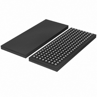
SSTUG32868ET/G,518 NXP Semiconductors, SSTUG32868ET/G,518 Datasheet - Page 8

SSTUG32868ET/G,518
Manufacturer Part Number
SSTUG32868ET/G,518
Description
IC BUFFER 1.8V 25BIT 176-LFBGA
Manufacturer
NXP Semiconductors
Datasheet
1.SSTUG32868ETG518.pdf
(29 pages)
Specifications of SSTUG32868ET/G,518
Logic Type
1:2 Configurable Registered Buffer with Parity
Supply Voltage
1.7 V ~ 2 V
Number Of Bits
28
Operating Temperature
0°C ~ 70°C
Mounting Type
Surface Mount
Package / Case
176-TFBGA
Lead Free Status / RoHS Status
Lead free / RoHS Compliant
Other names
935284276518
SSTUG32868ET/G-T
SSTUG32868ET/G-T
SSTUG32868ET/G-T
SSTUG32868ET/G-T
Available stocks
Company
Part Number
Manufacturer
Quantity
Price
Company:
Part Number:
SSTUG32868ET/G,518
Manufacturer:
NXP Semiconductors
Quantity:
10 000
NXP Semiconductors
Table 3.
SSTUG32868_1
Product data sheet
Symbol
Ungated inputs
DCKE0
DCKE1
DODT0
DODT1
Chip Select gated inputs
D1 to
D28
Chip Select inputs
DCS0
DCS1
DCS2
DCS3
Configuration control inputs
C
Re-driven outputs
Q1A to
Q28A
Q1B to
Q28B
QCS0A
QCS0B
QCS1A
QCS1B
Pin
1 : 2 Register A (C = 0)
D1
C1
N1
P1
A2, A1, B2, B1, C2, C1,
D2, D1, E1, F1, G1, H1,
N1, P1, R1, T1, U1, V1,
W1, W2, Y1, Y2, AA1,
AA2, AB1, AB2
K1
J1
K3
P3
A3
A7, B7, C7, D7, E7, E2, F7,
F2, G7, G2, H7, H2, N2,
P2, R2, R7, T2, T7, U2,
U7, V2, V7, W7, Y7, AA7,
AB7
A8, B8, C8, D8, E8, F8,
G8, H8, J8, J7, K8, K7, L8,
L7, M7, M8, N7, N8, P7,
P8, R8, T8, V8, U8, W8,
Y8, AA8, AB8
K2
L7
J2
L8
Pin description
6.2 Pin description
1 : 2 Register B (C = 1)
W1
Y1
K1
J1
A2, A1, B2, B1, C2, C1,
D2, D1, E1, F1, G1, H1, J1,
K1, N1, P1, R1, T1, U1,
V1, W1, W2, Y1, Y2, AA1,
AA2, AB1, AB2
N1
P1
K3
P3
A3
A7, B7, C7, D7, E7, E2, F7,
F2, G7, G2, H7, H2, J2,
K2, N2, P2, R2, R7, T2, T7,
U2, U7, V2, V7, W7, Y7,
AA7, AB7
A8, B8, C8, D8, E8, F8,
G8, H8, J8, J7, K8, K7, L8,
L7, M7, M8, N7, N8, P7,
P8, R8, T8, U8, V8, W8,
Y8, AA8, AB8
N2
M7
P2
M8
Rev. 01 — 23 April 2007
1.8 V DDR2-1G configurable registered buffer with parity
Type
SSTL_18
SSTL_18
SSTL_18
SSTL_18
LVCMOS
input
1.8 V
CMOS
outputs
1.8 V
CMOS
outputs
Description
The outputs of this register will not be
suspended by the DCS0 and DCS1
control.
The outputs of this register will not be
suspended by the DCS0 and DCS1
control.
Data inputs, clocked in on the crossing of
the rising edge of CK and the falling
edge of CK.
Chip select inputs. These pins initiate
DRAM address/command decodes, and
as such at least one will be LOW when a
valid address/command is present. The
register can be programmed to re-drive
all D-inputs (CSGEN = HIGH) only when
at least one chip select input is LOW. If
CSGEN, DCS0 and DCS1 inputs are
HIGH, D1 to D28
disabled.
Configuration control inputs; Register A
or Register B
Data outputs
the DCS0 and DCS1 control.
Data outputs that will not be suspended
by the DCS0 and DCS1 control.
SSTUG32868
[2]
that are suspended by
[1]
inputs will be
© NXP B.V. 2007. All rights reserved.
8 of 29


