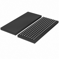
SSTUG32868ET/G,518 NXP Semiconductors, SSTUG32868ET/G,518 Datasheet - Page 11

SSTUG32868ET/G,518
Manufacturer Part Number
SSTUG32868ET/G,518
Description
IC BUFFER 1.8V 25BIT 176-LFBGA
Manufacturer
NXP Semiconductors
Datasheet
1.SSTUG32868ETG518.pdf
(29 pages)
Specifications of SSTUG32868ET/G,518
Logic Type
1:2 Configurable Registered Buffer with Parity
Supply Voltage
1.7 V ~ 2 V
Number Of Bits
28
Operating Temperature
0°C ~ 70°C
Mounting Type
Surface Mount
Package / Case
176-TFBGA
Lead Free Status / RoHS Status
Lead free / RoHS Compliant
Other names
935284276518
SSTUG32868ET/G-T
SSTUG32868ET/G-T
SSTUG32868ET/G-T
SSTUG32868ET/G-T
Available stocks
Company
Part Number
Manufacturer
Quantity
Price
Company:
Part Number:
SSTUG32868ET/G,518
Manufacturer:
NXP Semiconductors
Quantity:
10 000
NXP Semiconductors
Table 5.
[1]
[2]
[3]
[4]
[5]
SSTUG32868_1
Product data sheet
RESET
DCS2 and DCS3 operate identically to DCS0 and DCS1 with regard to the parity function.
PAR_IN arrives one clock cycle after the data to which it applies.
This transition assumes QERR is HIGH at the crossing of CK going HIGH and CK going LOW. If QERR is LOW, it stays latched LOW for
two clock cycles or until RESET is driven LOW.
QERR
If DCS0, DCS1, DCS2, DCS3 and CSGEN are driven HIGH, the device is placed in Low-Power Mode (LPM). If a parity error occurs on
the clock cycle before the device enters the LPM and the QERR output is driven LOW, it stays latched LOW for the LPM duration plus
two clock cycles or until RESET is driven LOW.
H
H
H
H
H
H
H
H
H
H
L
0
is the previous state of output QERR.
Parity and standby function table
X or floating
DCS0
7.2 Functional information
X
X
X
X
H
X
L
L
L
L
[1]
The SSTUG32868 is a 28-bit 1 : 2 configurable registered buffer designed for 1.7 V to
1.9 V V
All inputs are compatible with the JEDEC standard for SSTL_18, except the chip-select
gate-enable (CSGEN), control (C), and reset (RESET) inputs, which are LVCMOS. All
outputs are edge-controlled circuits optimized for unterminated DIMM loads, and meet
SSTL_18 specifications, except the open-drain error (QERR) output.
The device supports low-power standby operation. When RESET is LOW, the differential
input receivers are disabled, and undriven (floating) data, clock, and reference voltage
(VREF) inputs are allowed. In addition, when RESET is LOW, all registers are reset and
all outputs are forced LOW except QERR. The LVCMOS RESET and C inputs always
must be held at a valid logic HIGH or LOW level.
To ensure defined outputs from the register before a stable clock has been supplied,
RESET must be held in the LOW state during power-up.
In the DDR2 RDIMM application, RESET is specified to be completely asynchronous with
respect to CK and CK. Therefore, no timing relationship can be ensured between the two.
When entering reset, the register will be cleared and the data outputs will be driven LOW
quickly, relative to the time to disable the differential input receivers. However, when
coming out of reset, the register will become active quickly, relative to the time to enable
the differential input receivers. As long as the data inputs are LOW, and the clock is stable
X or floating
DCS1
DD
H
X
X
X
X
X
L
L
L
L
[1]
operation.
X or floating
L or H
CK
Inputs
Rev. 01 — 23 April 2007
1.8 V DDR2-1G configurable registered buffer with parity
X or floating
L or H
CK
(D1 to D28)
of inputs = H
even
even
even
even
odd
odd
odd
odd
X
X
X
SSTUG32868
X or floating
PAR_IN
H
H
H
H
L
L
L
L
X
X
[2]
© NXP B.V. 2007. All rights reserved.
QERR
QERR
Output
QERR
H
H
H
H
H
L
L
L
L
[3][4]
11 of 29
0
[5]
0


