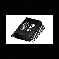
BUK9MJJ-65PLL NXP Semiconductors, BUK9MJJ-65PLL Datasheet - Page 5

BUK9MJJ-65PLL
Manufacturer Part Number
BUK9MJJ-65PLL
Description
Dual N-channel enhancement mode field-effect power transistor in SO20
Manufacturer
NXP Semiconductors
Datasheet
1.BUK9MJJ-65PLL.pdf
(16 pages)
NXP Semiconductors
5. Thermal characteristics
Table 5.
BUK9MJJ-65PLL
Product data sheet
Symbol
R
R
Fig 4.
th(j-sp)
th(j-a)
Safe operating area; continuous and peak drain currents as a function of drain-source voltage
Thermal characteristics
Parameter
thermal resistance
from junction to solder
point
thermal resistance
from junction to
ambient
(A)
I
10
10
D
10
10
10
−1
−2
1
3
2
10
−1
Conditions
FET1
FET2
mounted on a printed-circuit board; both
channels conducting; zero heat sink
area; see
mounted on a printed-circuit board; both
channels conducting; 200 mm² copper
heat sink area; see
mounted on a printed-circuit board; both
channels conducting; 400 mm² copper
heat sink area; see
mounted on a printed-circuit board; one
channel conducting; zero heat sink
area; see
mounted on a printed-circuit board; one
channel conducting; 200 mm² copper
heat sink area; see
mounted on a printed-circuit board; one
channel conducting; 400 mm² copper
heat sink area; see
All information provided in this document is subject to legal disclaimers.
Limit R
DSon
1
Rev. 03 — 15 July 2010
Figure 5
Figure 5
= V
DS
/ I
D
Figure 6
Figure 7
Figure 6
Figure 7
DC
10
Dual TrenchPLUS FET Logic Level FET
V
BUK9MJJ-65PLL
DS
(V)
001aal758
Min
-
-
-
-
-
-
-
-
t
10 ms
100 μs
1 ms
100 ms
p
= 10 μs
10
2
Typ
-
-
73
60
51
105
90
70
© NXP B.V. 2010. All rights reserved.
Max
28
28
-
-
-
-
-
-
Unit
K/W
K/W
K/W
K/W
K/W
K/W
K/W
K/W
5 of 16


