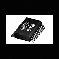
BUK9MJJ-65PLL NXP Semiconductors, BUK9MJJ-65PLL Datasheet - Page 10

BUK9MJJ-65PLL
Manufacturer Part Number
BUK9MJJ-65PLL
Description
Dual N-channel enhancement mode field-effect power transistor in SO20
Manufacturer
NXP Semiconductors
Datasheet
1.BUK9MJJ-65PLL.pdf
(16 pages)
NXP Semiconductors
BUK9MJJ-65PLL
Product data sheet
Fig 15. Normalized drain-source on-state resistance
Fig 17. Ratio of drain current to sense current as a
I
D
/ I
7000
6500
6000
5500
5000
4500
sense
a
2.0
1.5
1.0
0.5
0
-60
factor as a function of junction temperature,
FET1 and FET2
function of gate-source voltage; typical values,
FET1 and FET2
2
0
4
60
6
120
8
All information provided in this document is subject to legal disclaimers.
V
T
001aal629
001aal630
GS
j
(°C)
(V)
180
10
Rev. 03 — 15 July 2010
Fig 16. Drain-source on-state resistance as a function
Fig 18. Temperature sense diode forward voltage as a
V
F(TS D)
R
(mΩ)
DSon
100
80
60
40
20
0
4
3
2
1
of drain current; typical values, FET1 and FET2
function of junction temperature; typical
values, FET1 and FET2
0
0
2.5
Dual TrenchPLUS FET Logic Level FET
3.0
30
BUK9MJJ-65PLL
50
3.5
60
4.0
100
4.5
V
90
GS
© NXP B.V. 2010. All rights reserved.
003a a d914
003aae494
(V) = 10
I
T
D
j
(A)
( C)
5.0
150
120
10 of 16


