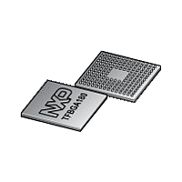
LPC3130_3131 NXP Semiconductors, LPC3130_3131 Datasheet - Page 35

LPC3130_3131
Manufacturer Part Number
LPC3130_3131
Description
The NXP LPC3130/3131 combine an 180 MHz ARM926EJ-S CPU core, high-speed USB2
Manufacturer
NXP Semiconductors
Datasheet
1.LPC3130_3131.pdf
(68 pages)
- Current page: 35 of 68
- Download datasheet (301Kb)
NXP Semiconductors
LPC3130_3131_1
Preliminary data sheet
6.29 System control registers
6.30 I2S0/1 interfaces
The System Control Registers (SysCReg) module provides a register interface for some
of the high-level settings in the system such as multiplexers and mode settings. This is an
auxiliary module included in this overview for the sake of completeness.
The I2S0/1 receive and I2S0/1 transmit modules have the following features:
•
•
•
•
•
•
•
•
•
•
•
•
Audio interface compatible with the I
I2S0/1 receive supports master mode and slave mode.
I2S0/1 transmit supports master mode.
Supports LSB justified words of 16, 18, 20 and 24 bits.
Supports a configurable number of bit clock periods per Word Select period (up to
128 bit clock periods).
Supports DMA transfers.
Transmit FIFO (I
Supports single 16 bit transfers to/from the left or right FIFO.
Supports single 24 bit transfers to/from the left or right FIFO.
Supports 32-bit interleaved transfers, with the lower 16 bits representing the left audio
sample, and the higher 16 bits representing the right audio sample.
Supports two 16-bit audio samples combined in a 32-bit word (2 left or 2 right
samples) to reduce busload.
Provides maskable interrupts for audio status: FIFO underrun/overrun/full/
half_full/not empty for left and right channel separately.
2
S transmit) or receive FIFO (I
Rev. 1 — 9 February 2009
Low-cost, low-power ARM926EJ-S microcontrollers
2
S standard.
2
S receive) of 4 stereo samples.
LPC3130/3131
© NXP B.V. 2009. All rights reserved.
35 of 68
Related parts for LPC3130_3131
Image
Part Number
Description
Manufacturer
Datasheet
Request
R

Part Number:
Description:
Manufacturer:
Philips Semiconductors (Acquired by NXP)
Datasheet:
Part Number:
Description:
NXP Semiconductors designed the LPC2420/2460 microcontroller around a 16-bit/32-bitARM7TDMI-S CPU core with real-time debug interfaces that include both JTAG andembedded trace
Manufacturer:
NXP Semiconductors
Datasheet:

Part Number:
Description:
NXP Semiconductors designed the LPC2458 microcontroller around a 16-bit/32-bitARM7TDMI-S CPU core with real-time debug interfaces that include both JTAG andembedded trace
Manufacturer:
NXP Semiconductors
Datasheet:
Part Number:
Description:
NXP Semiconductors designed the LPC2468 microcontroller around a 16-bit/32-bitARM7TDMI-S CPU core with real-time debug interfaces that include both JTAG andembedded trace
Manufacturer:
NXP Semiconductors
Datasheet:
Part Number:
Description:
NXP Semiconductors designed the LPC2470 microcontroller, powered by theARM7TDMI-S core, to be a highly integrated microcontroller for a wide range ofapplications that require advanced communications and high quality graphic displays
Manufacturer:
NXP Semiconductors
Datasheet:
Part Number:
Description:
NXP Semiconductors designed the LPC2478 microcontroller, powered by theARM7TDMI-S core, to be a highly integrated microcontroller for a wide range ofapplications that require advanced communications and high quality graphic displays
Manufacturer:
NXP Semiconductors
Datasheet:
Part Number:
Description:
The Philips Semiconductors XA (eXtended Architecture) family of 16-bit single-chip microcontrollers is powerful enough to easily handle the requirements of high performance embedded applications, yet inexpensive enough to compete in the market for hi
Manufacturer:
NXP Semiconductors
Datasheet:
Part Number:
Description:
The XA-S3 device is a member of Philips Semiconductors? XA(eXtended Architecture) family of high performance 16-bitsingle-chip microcontrollers
Manufacturer:
NXP Semiconductors
Datasheet:

Part Number:
Description:
The NXP BlueStreak LH75401/LH75411 family consists of two low-cost 16/32-bit System-on-Chip (SoC) devices
Manufacturer:
NXP Semiconductors
Datasheet:

Part Number:
Description:
The NXP LPC3141 combine a 270 MHz ARM926EJ-S CPU core, High-speed USB 2
Manufacturer:
NXP Semiconductors

Part Number:
Description:
The NXP LPC3143 combine a 270 MHz ARM926EJ-S CPU core, High-speed USB 2
Manufacturer:
NXP Semiconductors

Part Number:
Description:
The NXP LPC3152 combines an 180 MHz ARM926EJ-S CPU core, High-speed USB 2
Manufacturer:
NXP Semiconductors

Part Number:
Description:
The NXP LPC3154 combines an 180 MHz ARM926EJ-S CPU core, High-speed USB 2
Manufacturer:
NXP Semiconductors

Part Number:
Description:
Standard level N-channel enhancement mode Field-Effect Transistor (FET) in a plastic package using NXP High-Performance Automotive (HPA) TrenchMOS technology
Manufacturer:
NXP Semiconductors
Datasheet:


