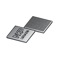
LPC1850FET256 NXP Semiconductors, LPC1850FET256 Datasheet - Page 74

LPC1850FET256
Manufacturer Part Number
LPC1850FET256
Description
The LPC1850FET256 is a high-performance, cost-effective Cortex-M3 microcontroller featuring 200 kB of SRAM, and advanced peripherals including Ethernet, High Speed USB 2
Manufacturer
NXP Semiconductors
Datasheet
1.LPC1810FBD144.pdf
(157 pages)
Available stocks
Company
Part Number
Manufacturer
Quantity
Price
Company:
Part Number:
LPC1850FET256
Manufacturer:
NXP
Quantity:
1 000
Part Number:
LPC1850FET256
Manufacturer:
NXP/恩智浦
Quantity:
20 000
Company:
Part Number:
LPC1850FET256,551
Manufacturer:
NXP Semiconductors
Quantity:
10 000
Part Number:
LPC1850FET256,551
Manufacturer:
NXP/恩智浦
Quantity:
20 000
NXP Semiconductors
LPC1850_30_20_10
Preliminary data sheet
7.11.1.1 Features
7.12.1 Features
7.11.1 AES decryption
7.11.2 One-Time Programmable (OTP) memory
7.12 General Purpose I/O (GPIO)
7.11 Decryption features
The hardware AES decryption can decode data using the AES algorithm in conjunction
with a 128-bit key.
The OTP provides 128 bit of memory for general purpose use and two 128-bit non-volatile
memory blocks to store AES keys or other customer data.
The LPC1850/30/20/10 provides eight GPIO ports with up to 31 GPIO pins each.
Device pins that are not connected to a specific peripheral function are controlled by the
GPIO registers. Pins may be dynamically configured as inputs or outputs. Separate
registers allow setting or clearing any number of outputs simultaneously. The value of the
output register may be read back as well as the current state of the port pins.
All GPIO pins default to inputs with pull-up resistors enabled on reset.
•
•
•
•
•
•
•
•
•
•
•
Decoding of external flash data connected to the quad SPI Flash Interface (SPIFI).
Secure storage of keys.
Support for CMAC hash calculation to authenticate encrypted data.
Data is processed in little endian mode. This means that the first byte read from flash
is integrated into the AES codeword as least significant byte. The 16th byte read from
flash is the most significant byte of the first AES codeword.
AES engine performance of 1 byte/clock cycle.
DMA transfers supported through the GPDMA.
Accelerated GPIO functions:
– GPIO registers are located on the AHB so that the fastest possible I/O timing can
– Mask registers allow treating sets of port bits as a group, leaving other bits
– All GPIO registers are byte and half-word addressable.
– Entire port value can be written in one instruction.
Bit-level set and clear registers allow a single instruction set or clear of any number of
bits in one port.
Direction control of individual bits.
All I/O default to inputs after reset.
Up to eight GPIO pins can be selected from all GPIO pins to create an edge- or
level-sensitive GPIO interrupt request.
be achieved.
unchanged.
All information provided in this document is subject to legal disclaimers.
Rev. 3.1 — 15 December 2011
32-bit ARM Cortex-M3 microcontroller
LPC1850/30/20/10
© NXP B.V. 2011. All rights reserved.
74 of 157


