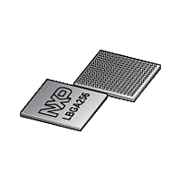
LPC1850FET256 NXP Semiconductors, LPC1850FET256 Datasheet - Page 66

LPC1850FET256
Manufacturer Part Number
LPC1850FET256
Description
The LPC1850FET256 is a high-performance, cost-effective Cortex-M3 microcontroller featuring 200 kB of SRAM, and advanced peripherals including Ethernet, High Speed USB 2
Manufacturer
NXP Semiconductors
Datasheet
1.LPC1810FBD144.pdf
(157 pages)
Available stocks
Company
Part Number
Manufacturer
Quantity
Price
Company:
Part Number:
LPC1850FET256
Manufacturer:
NXP
Quantity:
1 000
Part Number:
LPC1850FET256
Manufacturer:
NXP/恩智浦
Quantity:
20 000
Company:
Part Number:
LPC1850FET256,551
Manufacturer:
NXP Semiconductors
Quantity:
10 000
Part Number:
LPC1850FET256,551
Manufacturer:
NXP/恩智浦
Quantity:
20 000
NXP Semiconductors
[3]
[4]
[5]
[6]
[7]
[8]
[9]
[10] Pad provides USB functions. 5 V tolerant if V
[11] Open-drain 5 V tolerant digital I/O pad, compatible with I
[12] 5 V tolerant pad with 20 ns glitch filter; provides digital I/O functions with open-drain output with weak pull-up resistor and hysteresis
[13] On the TFBGA100 and LQFP208 packages, VPP is internally connected to VDDIO.
[14] On the LQFP144/208 packages, VSSIO and VSS are connected to a common ground plane.
[15] On the TFBGA100 and LQFP100/208 packages, VSS is internally connected to VSSIO.
LPC1850_30_20_10
Preliminary data sheet
5 V tolerant pad with 15 ns glitch filter (5 V tolerant if V
functions with TTL levels and hysteresis; normal drive strength (see
5 V tolerant pad with 15 ns glitch filter (5 V tolerant if V
functions with TTL levels, and hysteresis; high drive strength (see
5 V tolerant pad with 15 ns glitch filter (5 V tolerant if V
digital I/O functions with TTL levels and hysteresis (see
5 V tolerant pad providing digital I/O functions (with TTL levels and hysteresis) and analog input or output (5 V tolerant if V
if V
section of the pad must be disabled by setting the pin to an input function and disabling the pull-up resistor through the pin’s SFSP
register.
5 V tolerant transparent analog pad.
For maximum load C
5 V to VBUS = 0.2 V when it is no longer driven.
Transparent analog pad. Not 5 V tolerant.
the USB specification, revision 2.0 (Full-speed and Low-speed mode only).
provide output functionality. When power is switched off, this pin connected to the I
(see
DD(IO)
Figure
not present, do not exceed 3.3 V). When configured as a ADC input or DAC output, the pin is not 5 V tolerant and the digital
40).
L
= 6.5 F and maximum pull-down resistance R
All information provided in this document is subject to legal disclaimers.
DD(IO)
Rev. 3.1 — 15 December 2011
present; if V
DD(IO)
DD(IO)
DD(IO)
Figure
2
C-bus Fast Mode Plus specification. This pad requires an external pull-up to
present; if V
present; if V
present; if V
DD(IO)
39).
Figure
Figure
not present do not exceed 3.3 V. It is designed in accordance with
pd
= 80 k, the VBUS signal takes about 2 s to fall from VBUS =
DD(IO)
DD(IO)
DD(IO)
39).
39).
not present, do not exceed 3.3 V); provides digital I/O
not present, do not exceed 3.3 V); provides digital I/O
not present, do not exceed 3.3 V); provides high-speed
2
C-bus is floating and does not disturb the I
32-bit ARM Cortex-M3 microcontroller
LPC1850/30/20/10
© NXP B.V. 2011. All rights reserved.
DD(IO)
66 of 157
2
present;
C lines.


