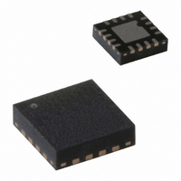
PCA9670BS,118 NXP Semiconductors, PCA9670BS,118 Datasheet - Page 9

PCA9670BS,118
Manufacturer Part Number
PCA9670BS,118
Description
IC I/O EXPANDER I2C 8B 16HVQFN
Manufacturer
NXP Semiconductors
Datasheet
1.PCA9670D518.pdf
(28 pages)
Specifications of PCA9670BS,118
Package / Case
16-VQFN Exposed Pad, 16-HVQFN, 16-SQFN, 16-DHVQFN
Interface
I²C
Number Of I /o
8
Interrupt Output
No
Frequency - Clock
1MHz
Voltage - Supply
2.3 V ~ 5.5 V
Operating Temperature
-40°C ~ 85°C
Mounting Type
Surface Mount
Includes
POR
Logic Family
PCA9670
Number Of Lines (input / Output)
8.0 / 8.0
Operating Supply Voltage
2.3 V to 5.5 V
Power Dissipation
400 mW
Operating Temperature Range
- 40 C to + 85 C
Input Voltage
5.5 V
Logic Type
I/O Expander
Maximum Clock Frequency
1 MHz
Mounting Style
SMD/SMT
Number Of Input Lines
8.0
Number Of Output Lines
8.0
Output Current
50 mA
Output Voltage
5.5 V
Lead Free Status / RoHS Status
Lead free / RoHS Compliant
Lead Free Status / RoHS Status
Lead free / RoHS Compliant, Lead free / RoHS Compliant
Other names
935282714118
PCA9670BS-T
PCA9670BS-T
PCA9670BS-T
PCA9670BS-T
NXP Semiconductors
PCA9670_2
Product data sheet
7.2.2 Device ID (PCA9670 ID field)
The I
a ‘Software Reset Abort’. The PCA9670 does not initiate a reset of its registers.
The unique sequence that initiates a Software Reset is described in
The Device ID field is a 3-byte read-only (24 bits) word giving the following information:
The Device ID is read-only, hardwired in the device and can be accessed as follows:
1. START command
2. The master sends the Reserved Device ID I
3. The master sends the I
4. The master sends a Re-START command.
5. The master sends the Reserved Device ID I
6. The device ID read can be done, starting with the 8 manufacturer bits (first byte +
7. The master ends the reading sequence by NACKing the last byte, thus resetting the
Fig 9. Software Reset sequence
•
•
•
8 bits with the manufacturer name, unique per manufacturer (for example, NXP).
13 bits with the part identification, assigned by manufacturer, the 7 MSBs with the
category ID and the 6 LSBs with the feature ID (for example, for example PCA9670
16-bit quasi-output I/O expander).
3 bits with the die revision, assigned by manufacturer (for example, Rev X).
bit set to 0 (write).
The LSB is a ‘Don’t care’ value. Only one device must acknowledge this byte (the one
that has the I
Remark: A STOP command followed by a START command will reset the slave state
machine and the Device ID read cannot be performed.
Remark: A STOP command or a Re-START command followed by an access to
another slave device will reset the slave state machine and the Device ID read cannot
be performed.
bit set to 1 (read).
4 MSB of the second byte), followed by the 13 part identification bits and then the
3 die revision bits (3 LSB of the third byte).
slave device state machine and allowing the master to send the STOP command.
Remark: The reading of the Device ID can be stopped anytime by sending a NACK
command.
2
C-bus master must interpret a non-acknowledge from the PCA9670 (at any time) as
S
START condition
2
C-bus slave address).
SWRST Call I
0
0
Rev. 02 — 17 July 2007
0
2
C-bus slave address of the slave device it needs to identify.
2
0
C-bus address
0
Remote 8-bit I/O expander for Fm+ I
0
acknowledge
from slave(s)
0
R/W
0
Registers are set to default power-up values.
A
0
2
2
0
C-bus address ‘1111 100’ with the R/W
C-bus address ‘1111 100’ with the R/W
SWRST data = 06h
0
0
PCA9670 is(are) reset.
0
1
acknowledge
from slave(s)
1
0
002aac263
Figure
A
PCA9670
© NXP B.V. 2007. All rights reserved.
2
P
C-bus with reset
9.
9 of 28


