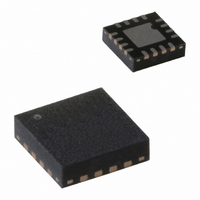
PCA9670BS,118 NXP Semiconductors, PCA9670BS,118 Datasheet - Page 8

PCA9670BS,118
Manufacturer Part Number
PCA9670BS,118
Description
IC I/O EXPANDER I2C 8B 16HVQFN
Manufacturer
NXP Semiconductors
Datasheet
1.PCA9670D518.pdf
(28 pages)
Specifications of PCA9670BS,118
Package / Case
16-VQFN Exposed Pad, 16-HVQFN, 16-SQFN, 16-DHVQFN
Interface
I²C
Number Of I /o
8
Interrupt Output
No
Frequency - Clock
1MHz
Voltage - Supply
2.3 V ~ 5.5 V
Operating Temperature
-40°C ~ 85°C
Mounting Type
Surface Mount
Includes
POR
Logic Family
PCA9670
Number Of Lines (input / Output)
8.0 / 8.0
Operating Supply Voltage
2.3 V to 5.5 V
Power Dissipation
400 mW
Operating Temperature Range
- 40 C to + 85 C
Input Voltage
5.5 V
Logic Type
I/O Expander
Maximum Clock Frequency
1 MHz
Mounting Style
SMD/SMT
Number Of Input Lines
8.0
Number Of Output Lines
8.0
Output Current
50 mA
Output Voltage
5.5 V
Lead Free Status / RoHS Status
Lead free / RoHS Compliant
Lead Free Status / RoHS Status
Lead free / RoHS Compliant, Lead free / RoHS Compliant
Other names
935282714118
PCA9670BS-T
PCA9670BS-T
PCA9670BS-T
PCA9670BS-T
NXP Semiconductors
PCA9670_2
Product data sheet
7.2.1 Software Reset
7.2 Software Reset Call, and device ID addresses
Two other different addresses can be sent to the PCA9670.
The Software Reset Call allows all the devices in the I
state value through a specific formatted I
implies that the I
The Software Reset sequence is defined as following:
1. A START command is sent by the I
2. The reserved General Call I
3. The PCA9670 device(s) acknowledge(s) after seeing the General Call address
4. Once the General Call address has been sent and acknowledged, the master sends
5. Once the right byte has been sent and correctly acknowledged, the master sends a
Fig 7. General Call address
Fig 8. Device ID address
•
•
General Call address: allows to reset the PCA9670 through the I
reception of the right I
information.
Device ID address: allows to read ID information from the device (manufacturer, part
identification, revision). See
information.
is sent by the I
‘0000 0000’ (00h) only. If the R/W bit is set to 1 (read), no acknowledge is returned to
the I
1 byte. The value of the byte must be equal to 06h.
a. The PCA9670 acknowledges this value only. If the byte is not equal to 06h, the
If more than 1 byte of data is sent, the PCA9670 does not acknowledge any more.
STOP command to end the Software Reset sequence: the PCA9670 then resets to
the default value (power-up value) and is ready to be addressed again within the
specified bus free time. If the master sends a Repeated START instead, no reset is
performed.
PCA9670 does not acknowledge it.
2
C-bus master.
2
C-bus is functional and that there is no device hanging the bus.
2
C-bus master.
Rev. 02 — 17 July 2007
2
C-bus sequence. See
0
1
2
Section 7.2.2 “Device ID (PCA9670 ID field)”
C-bus address ‘0000 000’ with the R/W bit set to 0 (write)
Remote 8-bit I/O expander for Fm+ I
0
1
0
1
2
C-bus master.
2
C-bus command. To be performed correctly, it
0
1
0
1
Section 7.2.1 “Software Reset”
0
0
002aac115
002aac116
2
0
0
C-bus to be reset to the power-up
R/W
R/W
0
2
C-bus upon
PCA9670
© NXP B.V. 2007. All rights reserved.
2
C-bus with reset
for more
for more
8 of 28


