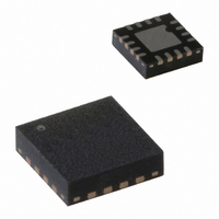
PCA9670BS,118 NXP Semiconductors, PCA9670BS,118 Datasheet - Page 5

PCA9670BS,118
Manufacturer Part Number
PCA9670BS,118
Description
IC I/O EXPANDER I2C 8B 16HVQFN
Manufacturer
NXP Semiconductors
Datasheet
1.PCA9670D518.pdf
(28 pages)
Specifications of PCA9670BS,118
Package / Case
16-VQFN Exposed Pad, 16-HVQFN, 16-SQFN, 16-DHVQFN
Interface
I²C
Number Of I /o
8
Interrupt Output
No
Frequency - Clock
1MHz
Voltage - Supply
2.3 V ~ 5.5 V
Operating Temperature
-40°C ~ 85°C
Mounting Type
Surface Mount
Includes
POR
Logic Family
PCA9670
Number Of Lines (input / Output)
8.0 / 8.0
Operating Supply Voltage
2.3 V to 5.5 V
Power Dissipation
400 mW
Operating Temperature Range
- 40 C to + 85 C
Input Voltage
5.5 V
Logic Type
I/O Expander
Maximum Clock Frequency
1 MHz
Mounting Style
SMD/SMT
Number Of Input Lines
8.0
Number Of Output Lines
8.0
Output Current
50 mA
Output Voltage
5.5 V
Lead Free Status / RoHS Status
Lead free / RoHS Compliant
Lead Free Status / RoHS Status
Lead free / RoHS Compliant, Lead free / RoHS Compliant
Other names
935282714118
PCA9670BS-T
PCA9670BS-T
PCA9670BS-T
PCA9670BS-T
NXP Semiconductors
7. Functional description
PCA9670_2
Product data sheet
7.1 Device address
Refer to
Following a START condition, the bus master must send the address of the slave it is
accessing and the operation it wants to perform (read or write). The address of the
PCA9670 is shown in
64 slave addresses. To conserve power, no internal pull-up resistors are incorporated on
AD2, AD1, and AD0. Address values depending on AD2, AD1, and AD0 can be found in
Table 3 “PCA9670 address
Remark: When using the PCA9670, reserved I
caution since they can interfere with:
The last bit of the first byte defines the operation to be performed. When set to logic 1 a
read is selected, while a logic 0 selects a write operation.
When AD2, AD1 and AD0 are held to V
applied.
Fig 6. PCA9670 address
•
•
•
“reserved for future use” I
1111 111)
slave devices that use the 10-bit addressing scheme (1111 0xx)
High speed mode (Hs-mode) master code (0000 1xx)
Figure 1 “Block diagram of
Figure
Rev. 02 — 17 July 2007
map”.
6. Slave address pins AD2, AD1, and AD0 choose 1 of
2
A6
C-bus addresses (0000 011, 1111 101, 1111 110,
Remote 8-bit I/O expander for Fm+ I
A5
PCA9670”.
programmable
slave address
A4
DD
A3
or V
A2
SS
2
C-bus addresses must be used with
, the same address as the PCF8574 is
A1
A0
002aab636
R/W
PCA9670
© NXP B.V. 2007. All rights reserved.
2
C-bus with reset
5 of 28


