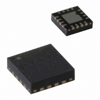
PCA9670BS,118 NXP Semiconductors, PCA9670BS,118 Datasheet - Page 12

PCA9670BS,118
Manufacturer Part Number
PCA9670BS,118
Description
IC I/O EXPANDER I2C 8B 16HVQFN
Manufacturer
NXP Semiconductors
Datasheet
1.PCA9670D518.pdf
(28 pages)
Specifications of PCA9670BS,118
Package / Case
16-VQFN Exposed Pad, 16-HVQFN, 16-SQFN, 16-DHVQFN
Interface
I²C
Number Of I /o
8
Interrupt Output
No
Frequency - Clock
1MHz
Voltage - Supply
2.3 V ~ 5.5 V
Operating Temperature
-40°C ~ 85°C
Mounting Type
Surface Mount
Includes
POR
Logic Family
PCA9670
Number Of Lines (input / Output)
8.0 / 8.0
Operating Supply Voltage
2.3 V to 5.5 V
Power Dissipation
400 mW
Operating Temperature Range
- 40 C to + 85 C
Input Voltage
5.5 V
Logic Type
I/O Expander
Maximum Clock Frequency
1 MHz
Mounting Style
SMD/SMT
Number Of Input Lines
8.0
Number Of Output Lines
8.0
Output Current
50 mA
Output Voltage
5.5 V
Lead Free Status / RoHS Status
Lead free / RoHS Compliant
Lead Free Status / RoHS Status
Lead free / RoHS Compliant, Lead free / RoHS Compliant
Other names
935282714118
PCA9670BS-T
PCA9670BS-T
PCA9670BS-T
PCA9670BS-T
NXP Semiconductors
PCA9670_2
Product data sheet
Fig 13. Read input port register
read from
data into
port
port
A LOW-to-HIGH transition of SDA while SCL is HIGH is defined as the STOP condition (P). Transfer of data can be stopped
at any moment by a STOP condition. When this occurs, data present at the last acknowledge phase is valid (Output mode).
Input data is lost.
SDA
8.3 Reading from a port (Input mode)
8.4 Power-on reset
8.5 RESET input
S A6
START condition
All ports programmed as input should be set to logic 1. To read, the master
(microcontroller) first addresses the slave device after it receives the interrupt. By setting
the last bit of the byte containing the slave address to logic 1 the Read mode is entered.
The data bytes that follow on the SDA are the values on the ports.
If the data on the input port changes faster than the master can read, this data may be
lost.
When power is applied to V
a reset condition until V
and the PCA9670 registers and I
states. Thereafter V
A reset can be accomplished by holding the RESET pin LOW for a minimum of t
PCA9670 registers and I
RESET input is once again HIGH.
A5 A4 A3 A2 A1 A0 1
slave address
t
h(D)
R/W
DD
A
acknowledge
from slave
must be lowered below 0.2 V to reset the device.
DD
Rev. 02 — 17 July 2007
2
C-bus state machine will be held in their default state until the
has reached V
DD
DATA 2
, an internal Power-On Reset (POR) holds the PCA9670 in
data from port
DATA 1
2
Remote 8-bit I/O expander for Fm+ I
C-bus/SMBus state machine will initialize to their default
DATA 3
t
su(D)
POR
. At that point, the reset condition is released
A
acknowledge
from master
data from port
DATA 4
DATA 4
PCA9670
© NXP B.V. 2007. All rights reserved.
2
C-bus with reset
1
no acknowledge
from master
002aac266
P
STOP
condition
w(rst)
12 of 28
. The


