PCA9670BS,118 NXP Semiconductors, PCA9670BS,118 Datasheet - Page 3
PCA9670BS,118
Manufacturer Part Number
PCA9670BS,118
Description
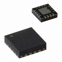
IC I/O EXPANDER I2C 8B 16HVQFN
Manufacturer
NXP Semiconductors
Datasheet
1.PCA9670D518.pdf
(28 pages)
Specifications of PCA9670BS,118
Package / Case
16-VQFN Exposed Pad, 16-HVQFN, 16-SQFN, 16-DHVQFN
Interface
I²C
Number Of I /o
8
Interrupt Output
No
Frequency - Clock
1MHz
Voltage - Supply
2.3 V ~ 5.5 V
Operating Temperature
-40°C ~ 85°C
Mounting Type
Surface Mount
Includes
POR
Logic Family
PCA9670
Number Of Lines (input / Output)
8.0 / 8.0
Operating Supply Voltage
2.3 V to 5.5 V
Power Dissipation
400 mW
Operating Temperature Range
- 40 C to + 85 C
Input Voltage
5.5 V
Logic Type
I/O Expander
Maximum Clock Frequency
1 MHz
Mounting Style
SMD/SMT
Number Of Input Lines
8.0
Number Of Output Lines
8.0
Output Current
50 mA
Output Voltage
5.5 V
Lead Free Status / RoHS Status
Lead free / RoHS Compliant
Lead Free Status / RoHS Status
Lead free / RoHS Compliant, Lead free / RoHS Compliant
Other names
935282714118
PCA9670BS-T
PCA9670BS-T
PCA9670BS-T
PCA9670BS-T


NXP Semiconductors
6. Pinning information
PCA9670_2
Product data sheet
6.1 Pinning
Fig 2. Simplified schematic diagram of P0 to P7
Fig 3. Pin configuration for SO16
Fig 5. Pin configuration for HVQFN16
data from Shift Register
AD0
AD1
AD2
V
data to Shift Register
P0
P1
P2
P3
SS
1
2
3
4
5
6
7
8
power-on reset
write pulse
read pulse
PCA9670D
002aac257
Rev. 02 — 17 July 2007
index area
terminal 1
16
15
14
13
12
11
10
9
AD2
D
CI
P0
P1
P2
Remote 8-bit I/O expander for Fm+ I
V
SDA
SCL
RESET
P7
P6
P5
P4
FF
S
DD
1
2
3
4
Q
Transparent top view
PCA9670BS
D
CI
FF
S
Fig 4. Pin configuration for TSSOP16
Q
AD0
AD1
AD2
V
I
trt(pu)
P0
P1
P2
P3
SS
1
2
3
4
5
6
7
8
12
11
10
9
100 A
002aac261
SCL
RESET
P7
P6
PCA9670PW
I
I
OH
OL
002aac109
002aac258
PCA9670
© NXP B.V. 2007. All rights reserved.
2
C-bus with reset
V
P0 to P7
V
to interrupt logic
DD
SS
16
15
14
13
12
11
10
9
V
SDA
SCL
RESET
P7
P6
P5
P4
DD
3 of 28
Related parts for PCA9670BS,118
Image
Part Number
Description
Manufacturer
Datasheet
Request
R

Part Number:
Description:
Pca9670 Remote 8-bit I/o Expander For Fm I?c-bus With Reset
Manufacturer:
NXP Semiconductors
Datasheet:
Part Number:
Description:
NXP Semiconductors designed the LPC2420/2460 microcontroller around a 16-bit/32-bitARM7TDMI-S CPU core with real-time debug interfaces that include both JTAG andembedded trace
Manufacturer:
NXP Semiconductors
Datasheet:

Part Number:
Description:
NXP Semiconductors designed the LPC2458 microcontroller around a 16-bit/32-bitARM7TDMI-S CPU core with real-time debug interfaces that include both JTAG andembedded trace
Manufacturer:
NXP Semiconductors
Datasheet:
Part Number:
Description:
NXP Semiconductors designed the LPC2468 microcontroller around a 16-bit/32-bitARM7TDMI-S CPU core with real-time debug interfaces that include both JTAG andembedded trace
Manufacturer:
NXP Semiconductors
Datasheet:
Part Number:
Description:
NXP Semiconductors designed the LPC2470 microcontroller, powered by theARM7TDMI-S core, to be a highly integrated microcontroller for a wide range ofapplications that require advanced communications and high quality graphic displays
Manufacturer:
NXP Semiconductors
Datasheet:
Part Number:
Description:
NXP Semiconductors designed the LPC2478 microcontroller, powered by theARM7TDMI-S core, to be a highly integrated microcontroller for a wide range ofapplications that require advanced communications and high quality graphic displays
Manufacturer:
NXP Semiconductors
Datasheet:
Part Number:
Description:
The Philips Semiconductors XA (eXtended Architecture) family of 16-bit single-chip microcontrollers is powerful enough to easily handle the requirements of high performance embedded applications, yet inexpensive enough to compete in the market for hi
Manufacturer:
NXP Semiconductors
Datasheet:
Part Number:
Description:
The XA-S3 device is a member of Philips Semiconductors? XA(eXtended Architecture) family of high performance 16-bitsingle-chip microcontrollers
Manufacturer:
NXP Semiconductors
Datasheet:

Part Number:
Description:
The NXP BlueStreak LH75401/LH75411 family consists of two low-cost 16/32-bit System-on-Chip (SoC) devices
Manufacturer:
NXP Semiconductors
Datasheet:
Part Number:
Description:
The NXP LPC3130/3131 combine an 180 MHz ARM926EJ-S CPU core, high-speed USB2
Manufacturer:
NXP Semiconductors
Datasheet:
Part Number:
Description:
The NXP LPC3141 combine a 270 MHz ARM926EJ-S CPU core, High-speed USB 2
Manufacturer:
NXP Semiconductors
Part Number:
Description:
The NXP LPC3143 combine a 270 MHz ARM926EJ-S CPU core, High-speed USB 2
Manufacturer:
NXP Semiconductors

Part Number:
Description:
The NXP LPC3152 combines an 180 MHz ARM926EJ-S CPU core, High-speed USB 2
Manufacturer:
NXP Semiconductors
Part Number:
Description:
The NXP LPC3154 combines an 180 MHz ARM926EJ-S CPU core, High-speed USB 2
Manufacturer:
NXP Semiconductors