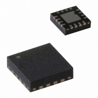
PCA9670BS,118 NXP Semiconductors, PCA9670BS,118 Datasheet - Page 17

PCA9670BS,118
Manufacturer Part Number
PCA9670BS,118
Description
IC I/O EXPANDER I2C 8B 16HVQFN
Manufacturer
NXP Semiconductors
Datasheet
1.PCA9670D518.pdf
(28 pages)
Specifications of PCA9670BS,118
Package / Case
16-VQFN Exposed Pad, 16-HVQFN, 16-SQFN, 16-DHVQFN
Interface
I²C
Number Of I /o
8
Interrupt Output
No
Frequency - Clock
1MHz
Voltage - Supply
2.3 V ~ 5.5 V
Operating Temperature
-40°C ~ 85°C
Mounting Type
Surface Mount
Includes
POR
Logic Family
PCA9670
Number Of Lines (input / Output)
8.0 / 8.0
Operating Supply Voltage
2.3 V to 5.5 V
Power Dissipation
400 mW
Operating Temperature Range
- 40 C to + 85 C
Input Voltage
5.5 V
Logic Type
I/O Expander
Maximum Clock Frequency
1 MHz
Mounting Style
SMD/SMT
Number Of Input Lines
8.0
Number Of Output Lines
8.0
Output Current
50 mA
Output Voltage
5.5 V
Lead Free Status / RoHS Status
Lead free / RoHS Compliant
Lead Free Status / RoHS Status
Lead free / RoHS Compliant, Lead free / RoHS Compliant
Other names
935282714118
PCA9670BS-T
PCA9670BS-T
PCA9670BS-T
PCA9670BS-T
NXP Semiconductors
12. Static characteristics
Table 5.
V
[1]
[2]
[3]
PCA9670_2
Product data sheet
Symbol
Supplies
V
I
I
V
Input SCL; input/output SDA
V
V
I
I
C
I/Os; P0 to P7
I
I
I
I
C
C
Input RESET
V
V
I
I
C
Inputs AD0, AD1, AD2
V
V
I
C
DD
stb
OL
L
OL
OL(tot)
OH
trt(pu)
LI
OH
LI
DD
DD
POR
IL
IH
IL
IH
IL
IH
i
i
o
i
i
= 2.3 V to 5.5 V; V
The power-on reset circuit resets the I
Each bit must be limited to a maximum of 25 mA and the total package limited to 200 mA due to internal busing limits.
The value is not tested, but verified on sampling basis.
Parameter
supply voltage
supply current
standby current
power-on reset voltage
LOW-level input voltage
HIGH-level input voltage
LOW-level output current
leakage current
input capacitance
LOW-level output current
total LOW-level output current
HIGH-level output current
transient boosted pull-up current V
input capacitance
output capacitance
LOW-level input voltage
HIGH-level input voltage
input leakage current
HIGH-level output current
input capacitance
LOW-level input voltage
HIGH-level input voltage
input leakage current
input capacitance
Static characteristics
SS
= 0 V; T
amb
[2]
= 40 C to +85 C; unless otherwise specified.
2
C-bus logic with V
[2]
Conditions
Operating mode; no load;
V
AD0, AD1, AD2 = static H or L
Standby mode; no load;
V
V
V
V
V
V
V
V
V
V
V
I
I
OL
OL
OL
I
I
OL
OL
OL
OL
OH
OH
= V
= V
= V
= V
= 0.4 V; V
= 0.4 V; V
= 0.4 V; V
= 0.5 V; V
= 0.5 V; V
= 0.5 V; V
= 0.5 V; V
= V
= V
Rev. 02 — 17 July 2007
DD
DD
DD
SS
SS
SS
or V
or V
or V
DD
; see
< V
SS
SS
SS
DD
DD
DD
DD
DD
DD
DD
POR
; f
; f
Remote 8-bit I/O expander for Fm+ I
Figure 12
SCL
SCL
= 2.3 V
= 3.0 V
= 4.5 V
= 2.3 V
= 3.0 V
= 4.5 V
= 4.5 V
and set all I/Os to logic 1 (with current source to V
= 1 MHz;
= 0 kHz
[1]
[3]
[3]
Min
2.3
-
-
-
0.7V
20
25
30
-
12
17
25
-
-
-
2
-
0.7V
-
0.5
1
30
0.5
0.5
1
1
0.5
1
DD
DD
Typ
-
266
2.5
1.8
-
-
-
-
-
-
4
27
35
41
-
3
3
-
-
-
-
3
-
-
-
3
250
1.0
PCA9670
© NXP B.V. 2007. All rights reserved.
2
C-bus with reset
Max
5.5
500
10
2.0
+0.3V
5.5
-
-
-
+1
10
-
-
-
200
-
10
10
+0.8
5.5
+1
+1
5
+0.3V
5.5
+1
5
300
DD
).
DD
DD
17 of 28
Unit
V
V
V
V
mA
mA
mA
pF
mA
mA
mA
mA
mA
pF
pF
V
V
pF
V
V
pF
A
A
A
A
A
A
A


