Si5369-EVB Silicon Laboratories Inc, Si5369-EVB Datasheet - Page 76
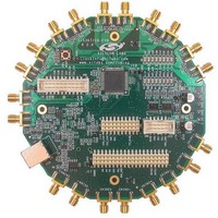
Si5369-EVB
Manufacturer Part Number
Si5369-EVB
Description
MCU, MPU & DSP Development Tools SI5369 DEV KIT
Manufacturer
Silicon Laboratories Inc
Specifications of Si5369-EVB
Processor To Be Evaluated
Si5369
Interface Type
I2C, SPI
Operating Supply Voltage
3.3 V
Lead Free Status / Rohs Status
Details


76
Note: Internal register names are indicated by underlined italics, e.g., INT_PIN. See Si5369 Register Map.
GND PAD
Pin #
77
78
82
83
87
88
90
92
93
97
98
CKOUT3+
CKOUT3–
CKOUT1–
CKOUT1+
CKOUT2+
CKOUT2–
CKOUT4–
CKOUT4+
Pin Name
FS_OUT–
FS_OUT+
GND PAD
CMODE
GND
Table 10. Si5369 Pin Descriptions (Continued)
I/O
O
O
O
O
O
I
Signal Level
LVCMOS
Supply
MULTI
MULTI
MULTI
MULTI
MULTI
Preliminary Rev. 0.4
Clock Output 3.
Differential clock output. Output signal format is selected by
SFOUT3_REG register bits. Output is differential for LVPECL,
LVDS, and CML compatible modes. For CMOS format, both
output pins drive identical single-ended clock outputs.
Clock Output 1.
Differential clock output. Output signal format is selected by
SFOUT1_REG register bits. Output is differential for LVPECL,
LVDS, and CML compatible modes. For CMOS format, both
output pins drive identical single-ended clock outputs.
Frame Sync Output.
Differential frame sync output or fifth high-speed clock output.
Output signal format is selected by SFOUT_FSYNC_REG reg-
ister bits. Output is differential for LVPECL, LVDS, and CML
compatible modes. For CMOS format, both output pins drive
identical single-ended clock outputs. Duty cycle and active
polarity are controlled by FSYNC_PW and FSYNC_POL bits,
respectively. Detailed operations and timing characteristics for
these pins may be found in the Any-Frequency Precision Clock
Family Reference Manual.
Control Mode.
Selects I
0 = I
1 = SPI Control Mode.
This pin must be tied high or low.
Clock Output 2.
Differential clock output. Output signal format is selected by
SFOUT2_REG register bits. Output is differential for LVPECL,
LVDS, and CML compatible modes. For CMOS format, both
output pins drive identical single-ended clock outputs.
Clock Output 4.
Differential clock output. Output signal format is selected by
SFOUT4_REG register bits. Output is differential for LVPECL,
LVDS, and CML compatible modes. For CMOS format, both
output pins drive identical single-ended clock outputs.
Ground Pad.
The ground pad must provide a low thermal and electrical
impedance to a ground plane.
2
C Control Mode.
2
C or SPI control mode for the device.
Description
Related parts for Si5369-EVB
Image
Part Number
Description
Manufacturer
Datasheet
Request
R

Part Number:
Description:
SMD/C°/SINGLE-ENDED OUTPUT SILICON OSCILLATOR
Manufacturer:
Silicon Laboratories Inc
Part Number:
Description:
Manufacturer:
Silicon Laboratories Inc
Datasheet:
Part Number:
Description:
N/A N/A/SI4010 AES KEYFOB DEMO WITH LCD RX
Manufacturer:
Silicon Laboratories Inc
Datasheet:
Part Number:
Description:
N/A N/A/SI4010 SIMPLIFIED KEY FOB DEMO WITH LED RX
Manufacturer:
Silicon Laboratories Inc
Datasheet:
Part Number:
Description:
N/A/-40 TO 85 OC/EZLINK MODULE; F930/4432 HIGH BAND (REV E/B1)
Manufacturer:
Silicon Laboratories Inc
Part Number:
Description:
EZLink Module; F930/4432 Low Band (rev e/B1)
Manufacturer:
Silicon Laboratories Inc
Part Number:
Description:
I°/4460 10 DBM RADIO TEST CARD 434 MHZ
Manufacturer:
Silicon Laboratories Inc
Part Number:
Description:
I°/4461 14 DBM RADIO TEST CARD 868 MHZ
Manufacturer:
Silicon Laboratories Inc
Part Number:
Description:
I°/4463 20 DBM RFSWITCH RADIO TEST CARD 460 MHZ
Manufacturer:
Silicon Laboratories Inc
Part Number:
Description:
I°/4463 20 DBM RADIO TEST CARD 868 MHZ
Manufacturer:
Silicon Laboratories Inc
Part Number:
Description:
I°/4463 27 DBM RADIO TEST CARD 868 MHZ
Manufacturer:
Silicon Laboratories Inc
Part Number:
Description:
I°/4463 SKYWORKS 30 DBM RADIO TEST CARD 915 MHZ
Manufacturer:
Silicon Laboratories Inc
Part Number:
Description:
N/A N/A/-40 TO 85 OC/4463 RFMD 30 DBM RADIO TEST CARD 915 MHZ
Manufacturer:
Silicon Laboratories Inc
Part Number:
Description:
I°/4463 20 DBM RADIO TEST CARD 169 MHZ
Manufacturer:
Silicon Laboratories Inc