Si5369-EVB Silicon Laboratories Inc, Si5369-EVB Datasheet - Page 74
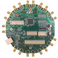
Si5369-EVB
Manufacturer Part Number
Si5369-EVB
Description
MCU, MPU & DSP Development Tools SI5369 DEV KIT
Manufacturer
Silicon Laboratories Inc
Specifications of Si5369-EVB
Processor To Be Evaluated
Si5369
Interface Type
I2C, SPI
Operating Supply Voltage
3.3 V
Lead Free Status / Rohs Status
Details


74
Note: Internal register names are indicated by underlined italics, e.g., INT_PIN. See Si5369 Register Map.
Pin #
13
57
16
17
29
30
32
42
34
35
39
40
44
45
Pin Name
CS0_C3A
CS1_C4A
CKIN4+
CKIN4–
CKIN2+
CKIN2–
CKIN3+
CKIN3–
CKIN1+
CKIN1–
RATE0
RATE1
XA
XB
Table 10. Si5369 Pin Descriptions (Continued)
I/O
I/O
I
I
I
I
I
I
Signal Level
LVCMOS
ANALOG
3-Level
MULTI
MULTI
MULTI
MULTI
Preliminary Rev. 0.4
Input Clock Select/CKIN3 or CKIN4 Active Clock Indicator.
Input: If manual clock selection is chosen, and if
CKSEL_PIN = 1, the CKSEL pins control clock selection and
the CKSEL_REG bits are ignored.
If CKSEL_PIN = 0, the CKSEL_REG register bits control this
function and these inputs tristate. If configured as inputs, these
pins must not float.
Output: If auto clock selection is enabled, then they serve as
the CKIN_n active clock indicator.
0 = CKIN3 (CKIN4) is not the active input clock
1 = CKIN3 (CKIN4) is currently the active input to the PLL
The CKn_ACTV_REG bit always reflects the active clock status
for CKIN_n. If CKn_ACTV_PIN = 1, this status will also be
reflected on the CnA pin with active polarity controlled by the
CK_ACTV_POL bit. If CKn_ACTV_PIN = 0, this output tristates.
External Crystal or Reference Clock.
External crystal should be connected to these pins to use inter-
nal oscillator based reference. Refer to Family Reference Man-
ual for interfacing to an external reference. External reference
must be from a high-quality clock source (TCXO, OCXO). Fre-
quency of crystal or external clock is set by the RATE pins.
Clock Input 4.
Differential clock input. This input can also be driven with a sin-
gle-ended signal. CKIN4 serves as the frame sync input associ-
ated with the CKIN2 clock when CK_CONFIG_REG = 1.
External Crystal or Reference Clock Rate.
Three level inputs that select the type and rate of external crys-
tal or reference clock to be applied to the XA/XB port. Refer to
the Family Reference Manual for settings. These pins have both
a weak pull-up and a weak pull-down; they default to M.
Clock Input 2.
Differential input clock. This input can also be driven with a sin-
gle-ended signal.
Clock Input 3.
Differential clock input. This input can also be driven with a sin-
gle-ended signal. CKIN3 serves as the frame sync input associ-
ated with the CKIN1 clock when CK_CONFIG_REG = 1.
Clock Input 1.
Differential clock input. This input can also be driven with a sin-
gle-ended signal.
CS[1:0]
00
01
10
11
Description
Active Input Clock
CKIN1
CKIN2
CKIN3
CKIN4
Related parts for Si5369-EVB
Image
Part Number
Description
Manufacturer
Datasheet
Request
R

Part Number:
Description:
SMD/C°/SINGLE-ENDED OUTPUT SILICON OSCILLATOR
Manufacturer:
Silicon Laboratories Inc
Part Number:
Description:
Manufacturer:
Silicon Laboratories Inc
Datasheet:
Part Number:
Description:
N/A N/A/SI4010 AES KEYFOB DEMO WITH LCD RX
Manufacturer:
Silicon Laboratories Inc
Datasheet:
Part Number:
Description:
N/A N/A/SI4010 SIMPLIFIED KEY FOB DEMO WITH LED RX
Manufacturer:
Silicon Laboratories Inc
Datasheet:
Part Number:
Description:
N/A/-40 TO 85 OC/EZLINK MODULE; F930/4432 HIGH BAND (REV E/B1)
Manufacturer:
Silicon Laboratories Inc
Part Number:
Description:
EZLink Module; F930/4432 Low Band (rev e/B1)
Manufacturer:
Silicon Laboratories Inc
Part Number:
Description:
I°/4460 10 DBM RADIO TEST CARD 434 MHZ
Manufacturer:
Silicon Laboratories Inc
Part Number:
Description:
I°/4461 14 DBM RADIO TEST CARD 868 MHZ
Manufacturer:
Silicon Laboratories Inc
Part Number:
Description:
I°/4463 20 DBM RFSWITCH RADIO TEST CARD 460 MHZ
Manufacturer:
Silicon Laboratories Inc
Part Number:
Description:
I°/4463 20 DBM RADIO TEST CARD 868 MHZ
Manufacturer:
Silicon Laboratories Inc
Part Number:
Description:
I°/4463 27 DBM RADIO TEST CARD 868 MHZ
Manufacturer:
Silicon Laboratories Inc
Part Number:
Description:
I°/4463 SKYWORKS 30 DBM RADIO TEST CARD 915 MHZ
Manufacturer:
Silicon Laboratories Inc
Part Number:
Description:
N/A N/A/-40 TO 85 OC/4463 RFMD 30 DBM RADIO TEST CARD 915 MHZ
Manufacturer:
Silicon Laboratories Inc
Part Number:
Description:
I°/4463 20 DBM RADIO TEST CARD 169 MHZ
Manufacturer:
Silicon Laboratories Inc